258 www.xilinx.com Virtex-5 RocketIO GTP Transceiver User Guide
UG196 (v1.3) May 25, 2007
Appendix A: MGT to GTP Transceiver Design Migration
R
Clocking
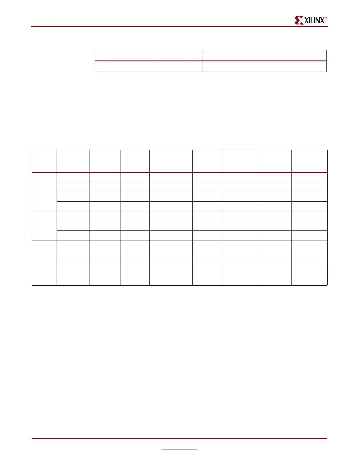
Virtex devices provide several available clock inputs. Table A-2 shows the clocks for each
family and their respective serial speeds.
Clock selection changed slightly across the first three generations of MGTs. In contrast, the
GTP_DUAL tile significantly enhances clocking capabilities by adding dedicated clocks
routing and MUXing resources. Figure A-1 shows how the reference clocks are selected for
each device.
Virtex-5 FPGA
(1)
8, 12, 16, 24
Notes:
1. Because two GTP transceivers use shared PLL resources in a GTP_DUAL tile, applications where
transceivers do not have common clock settings may not be able to use both transceivers in a tile. This
will reduce the total number of available transceivers in these applications.
Tab le A - 1 : Transceivers per Device (Continued)
Virtex Device # of Transceivers
Table A-2: Available Clock Inputs
Family
Clock
Names
Differential
(Internal)
Dedicated
Routes
Max Serial
Speeds (Gb/s)
Dynamic
Switching
Package
Input Voltage
(V)
(1)
Inputs per
Device
Clocks per
Device
Virtex-II
Pro
FPGA
BREFCLK Yes 3.125 Yes
(2)
2.5 8
(3)
2
(3)
BREFCLK2 Yes 3.125 Yes
(2)
2.5 8
(3)
2
(3)
REFCLK 2.5 Yes
(2)
2.5 8
(3)
2
(3)
REFCLK2 2.5 Yes
(2)
2.5 8
(3)
2
(3)
Virtex-4
FPGA
GREFCLK Yes Yes 1.0 Yes
(4)
Note 5 Note 5
REFCLK1 Yes Yes 6.5 Yes
(4)
84
REFCLK2 Yes Yes 6.5 Yes
(4)
84
Virtex-5
FPGA
GREFCLK Yes Yes Yes
1 per
GTP_DUAL
tile
1 per
GTP_DUAL
tile
REFCLK Yes Yes 3.125 Yes
1 per
GTP_DUAL
tile
1 per
GTP_DUAL
tile
Notes:
1. Nominal values. Refer to the specific data sheet for the exact values.
2. Dynamic selection between the REFCLKs or the BREFCLKs. To switch from REFCLK to BREFCLK or vice versa requires
reconfiguration.
3. BREFCLK should use dedicated GCLK I/O, which decreases GCLK I/O resources for other logic (also two pins per clock).
4. Reference clock switching is done via an attribute and the DRP using the RXAPMACLKSEL, RXBPMACLKSEL, and
TXABPMACLKSEL attributes. These attributes are located at DRP address 0x5D on bits [13:12], [11:10], and [9:8], respectively.
5. GREFCLK comes from the global clock tree and can come from any FPGA clock input. It should only be used for serial rates under
1.0 Gb/s.
 Loading...
