Digital I/O
Components in this discussion are located on the A1 circuit assembly
(34907-66501). The schematics are included in Chapter 8 starting on
page 261.
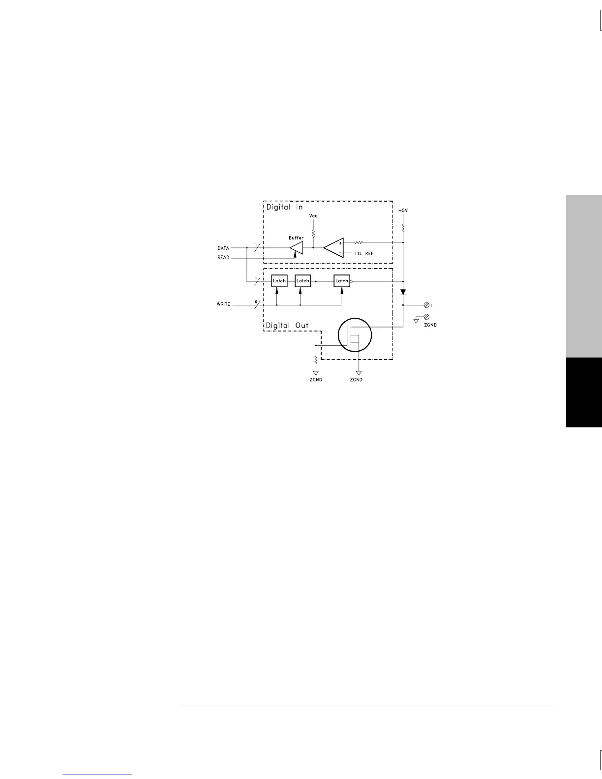
A simplified diagram of a digital I/O channel is shown below.
Two stages of latches on the outputs and one set of latches on the
inputs provide synchronous 16 bit writes and reads of the digital ports.
For digital output, data is written to the upper and lower bytes
(U201 and U202) separately, then latched into the output latches
U203 and U204 simultaneously. On a digital input data is latched
into the input latches U105 and U106 simultaneously.
MOSFETs are used to provide the low level output, and 74HC240’s
are used to provide the high level output.
During an output low, a logic high level is applied to the gate of the
MOSFET causing it to conduct and creating a low resistance path
from the data line to ZGND. In this state the MOSFET is capable of
sinking an externally supplied current of up to 400 mA. The blocking
diodes, CR301-CR308 and CR401-CR408 prevent any current from
sinking into the 74HC240’s.
During an output high, a logic low level is applied to the gate of the
MOSFET turning it off and presenting a high resistance between the
data line and ground.
Module Reference
5
Chapter 5 Theory of Operation
Multifunction Module
155
 Loading...