562 Chapter 16
W-CDMA Uplink Digital Modulation for Receiver Test
W-CDMA Uplink Concepts
Synchronization Diagrams
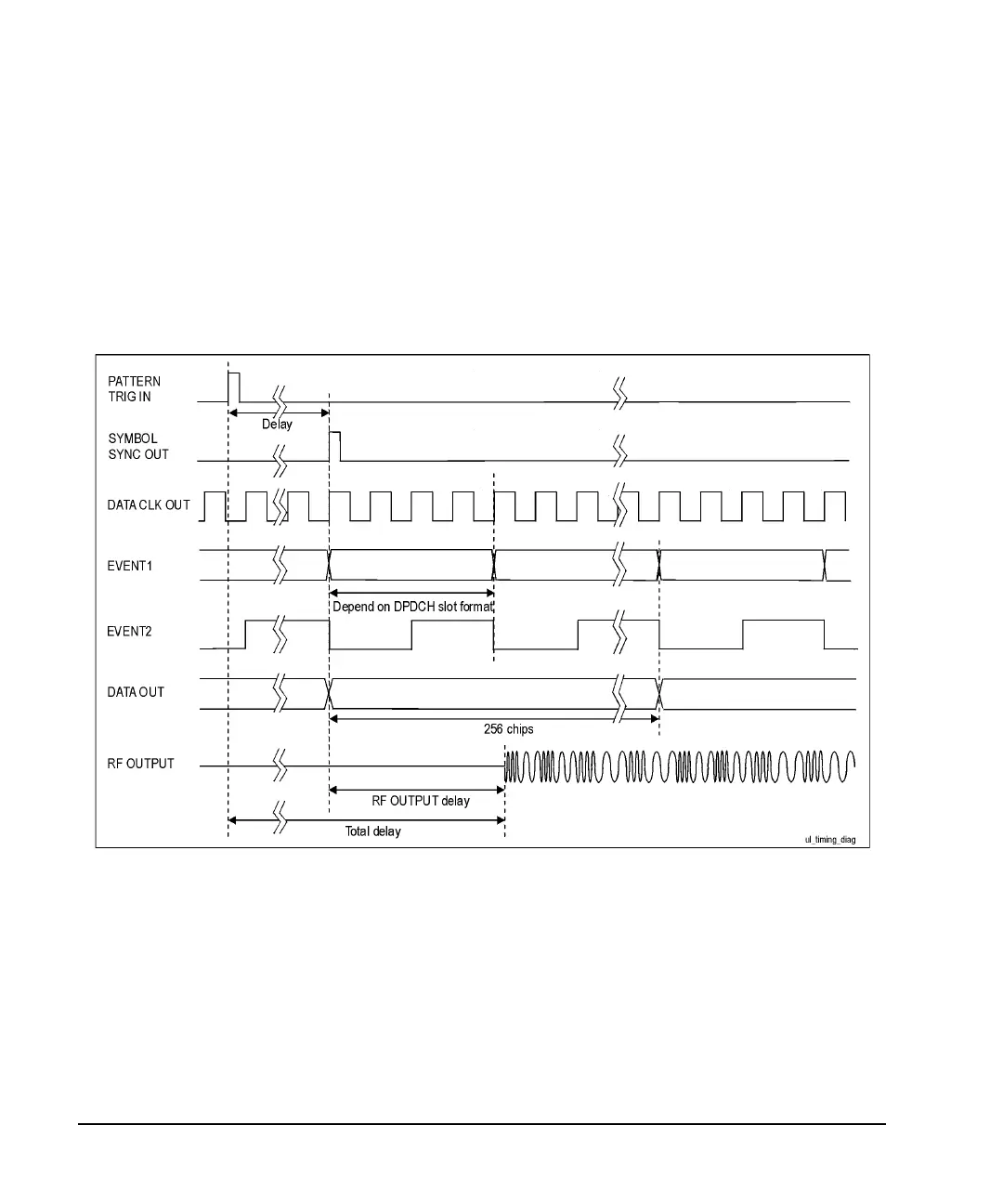
Signal Alignment for Default DPCH Mode
Figure 16-78 illustrates the timing relationships between the signals from the rear panel BNC input and
output connectors relative to the RF Output connector for default signal assignments in DPCH mode. Signal
states are referenced to the chip clock provided at the DATA CLK OUT connector.
Figure 16-78 Signal Alignment for Default DPCH Mode
DPCH Synchronization
Figure 16-79 illustrates the timing alignment for the DPCH channel. Delay time is defined by the sum of T0
(1024 chips = the standard timing offset between downlink and uplink), timing offset, and timeslot offset.
 Loading...