TS-990S
28
CIRCUIT DESCRIPTION
5-4. Transmit Power Control
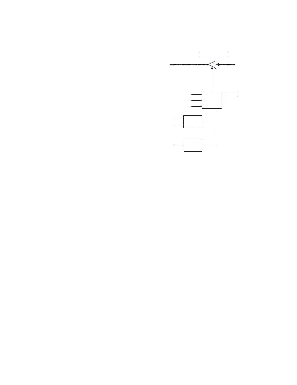
Transmit power control is done the same way as in previ-
ous models; the ALC circuit controls the ALC voltage using
the progressive wave voltage (VSF) and keeps a constant
output.
The voltage detected by the VSF/VSR detection circuit
(a circuit for the detection of progressive and refl ection wave
voltages) in the antenna switch unit (X53-441 A/2) is sent to
CN3 of the TX-RX unit (X57-827 A/2). The progressive wave
voltage is divided into a suitable voltage by the resistance,
and applied to the differential amplifi ers consisting of IC801.
The output voltage of IC801 (1/2) rises along with a rise
in progressive wave voltage while the base current of Q802
increases and the collector voltage, for which the ALC time
constant CR is selected, goes down. The output voltage of
the buffer (IC801 2/2) goes down along with a fall in collector
voltage. The resistance-distributed ALC voltage then goes
down. If the ALC voltage (2.5 V when the ALC is inactive)
goes down, the IF amplifier’s (Q706) second gate voltage
goes down and the gain is decreased.
When transmitting AM, Q801 is turned on approximately
50 ms after transmission, and the ALC voltage is controlled
by averaging the progressive wave voltage. The input voltage
into pin 2 of IC801 (1/2), which will be the ALC’s reference
voltage, is controlled by the adjustment value (POC) from
the main MCU, and sent from pin 5 of the D/A converter
(IC55).
SWR protection is controlled by the refl ection wave volt-
age. The refl ection wave voltage is divided by the resistance
and applied to IC802 (1/2). If it exceeds a specified volt-
age, the output of IC802 (1/2) increases the base current of
Q803, which performs ALC voltage control, thus lowering
the gain and power.
ID protection is under the control of the ID voltage detect-
ed in the fi nal circuit. The ID voltage is applied to IC802 (2/2).
If it exceeds a specifi ed voltage, the output of IC802 (2/2)
controls the ALC voltage and lowers the gain and power.
The PWR (power) meter is amplifi ed from the progressive
wave voltage, the SWR meter is amplifi ed from the refl ection
wave voltage, and the ALC meter is amplifi ed from the ALC
voltage by the relevant operation amplifi er, and they are ap-
plied to the ADC for meter-indication.
The VD meter indicates a divided drain voltage of the
fi nal circuit read by the A/D converter circuitry. The TEMP
meter for temperature protection uses the A/D converter
circuitry to read and display the voltages of the respective
thermistors (X45-388 A/2 TH1 and TH2) on the push-pull
FETs of the fi nal circuit and performs the three-stage (low-
, medium-, and high-speed) fan control of the fi nal unit and
two-stage (low- and high-speed) fan control of the AT unit.
If an abnormally high temperature occurs, the transceiver
lowers the transmit power to 5 W and displays a warning
message. If the temperature still rises, the transceiver stops
transmission and displays an error message.
The main screen displays each meter selected. Further-
more, the signals of meters selected in the configuration
menu can be sent out as MMET and SMET signals to ex-
ternal meters through the METER terminal and ACC2 ter-
minal. These signals are sent out from the D/A converter in
the main MCU, and IC101 in the TX-RX unit (X57-827 A/2)
6. Scope Circuit
6-1. From the IF Input Stage to the IF Amplifi er
(SCIF1_AMP)
The input signal into the scope circuit is an IF signal ob-
tained from the RX unit or the TX-RX unit, the frequency of
which is SC08M at the time of the main signal reception and
is set to SC11S or SC73S which varies with the reception
band at the time of the sub signal reception. And the scope
display is available at the time of signal transmission, the fre-
quency of which uses SC73S obtained from the TX-RX unit.
When SC08M and SC11S are selected, the signal is
amplified by the input buffer amplifier (Q7 and Q8). The
impedance is converted in L7 and L8 and sent to the next
stage via the diode switchers (D2 and D3). When SC73S is
selected, the input is amplifi ed by the input buffer amplifi er
(Q12) and sent to the next stage (SCIF1_BPF) via the diode
switcher (D4). SC73S does not pass along the 1st Mixer.
In the 1st mixer (SCMIX1), the signal is up converted by
SCLO1 (main: 61.721MHz/sub: 64.847MHz), and converted
to the 1st IF (SCIF1: 73.095MHz) for scope use. The SCIFI
signal passes through the BPF for the elimination of image
interference, and is sent to the IF amplifier (SCIF1_AMP)
via the attenuator. The attenuator provides three levels of at-
tenuation, -10 dB, -20 dB and -30 dB.
6-2. From the 2nd Mixer (SCMIX2) to the 3rd Mixer
(SCMIX3) Input
The SCIF1 is applied to the diode-employed DBM (2nd
mixer) and converted to the 2nd IF (SCIF2 at 10.7MHz). The
balanced-unbalanced conversion of the 2nd IF signal is per-
formed in L73 and transmitted to the MCF (XF1) on the next
stage. The output signal from the MCF is amplifi ed by the
SCIF2_AMP and sent to the SCMIX3 (3rd mixer).
Fig. 29 Transmit power control
makes level changes in the signals.
Q706
ALC
TX IF AMP (ALC)
VSF
POC
AMB
ALC
POWER
CONTROL
VSWR
PROTECT
ID
PROTECT
VSR
PRO
ID
Q803
IC802
EXT ALC
IC801(1/2)
Q802
IC801(2/2)
IC802
 Loading...