TS-990S
5
CIRCUIT DESCRIPTION
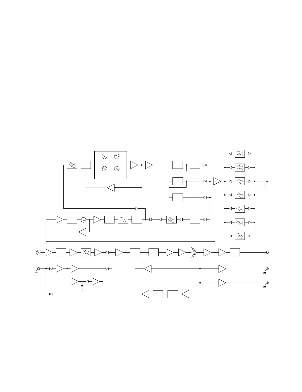
1-3. MLO1/MLO2
■
MLO1 (1st Local Oscillator for Main Receiver)
The VCO (Q4) oscillates at 393.6MHz. It is applied to pin
5 of the PLL (IC2) via the BPF. The 40MHz reference signal
is applied to pin 8. The signal which is applied to pin 5 of the
PLL (IC2) is frequency-divided by N and the reference signal
which is applied to pin 8 is frequency-divided by R. They are
phase-compared to lock the phase, and the phase-locked
393.6MHz signal is used as the reference of the DDS (IC3).
The output signal from the DDS (IC3) is amplifi ed by the
wide-band amplifi er (IC9). When using the DDS (IC3) output
directly as the MLO1, it is sent via the BPF, buffer (IC23),
amplifi er (Q99) and BPF. When using the VCO as the MLO1,
a signal which is amplifi ed by the wide-band amplifi er (IC9)
is applied to pin 8 of the PLL (IC17) via the BPF.
There are four VCOs (Q25, Q26, Q38 and Q39) for the
MLO1. They oscillate at 82.78 to 138.992MHz. These oscil-
lation outputs from the VCOs is applied to pin 5 of the PLL
(IC17). The signal which is applied to pin 5 is frequency-
divided by N and the signal which is applied to pin 8 is
frequency-divided by R. They are phase-compared to lock
the oscillating frequency, and used as a VCO output. The
oscillation output from the VCO is applied to the frequency
dividers (IC19, IC20, IC21 and IC22) via the amplifi er (Q45)
where the frequency is divided by 4, 8, or 10. The frequency
divided signal is passed through the amplifier (Q99) and
BPF, and is sent as the MLO1.
■
MLO2 (2nd Local Oscillator for Main Receiver)
The DDS (IC26) generates the MLO2 which is used
for the detector. The DDS (IC26) output signal is sent from
CN21 as the MLO2.
Fig. 2 Reference signal generator of the main receiver block, MLO1/MLO2
19.2M
X1
Q10
AMP
IC13
DDS
Buffer
CF1
Buffer
Q5
AMP
Q34
AMP
Q11
AMP
Q9
AMP
IC14D13
ERDET
CN33
10M
D19,20
D23,25
D7
AMP
Q46
IC18
PLL
X2
VCXO
20M
Q27
AMP
Q82
AMP
Q51
IC24
1/2
D28
R10M
Q3
AMP
IC2
PLL
393.6M
Q4
AMP
Q8
AMP
Q1
IC3
DDS
IC9
AMP
IC17
PLL
82.78~
92.48MHz
96.48~
107.48MHz
115.48~
128.992MHz
127.48~
138.992MHz
Q25, Q26, Q38, Q39
AMP
Q44
AMP
Q35
AMP
Q45
D12
D29
D33
Buffer
Q78
AMP
Q79
D49
Doubler
IC25
1/2
AMP
Q81
AMP
Q84
AMP
Q85
AMP
Q86
CN19
CN20
R40M
SCREF
AMP
Q80
IC26
DDS
CN21
MLO2
IC19
1/2
IC20
1/5
IC21
1/2
IC22
1/2
D39
D40
D38
D37
IC23
Buffer
D41
AMP
Q99
D43 D51
D44 D52
D45 D53
D46 D54
D47 D55
D48 D56
D42 D50
CN22
MLO1
 Loading...