Do you have a question about the Mitsubishi MELSEC-Q/L and is the answer not in the manual?
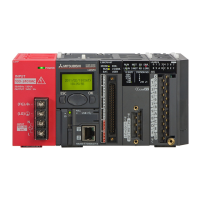
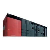
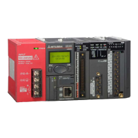
| Series | MELSEC-Q/L |
|---|---|
| Type | Programmable Logic Controller |
| Input Voltage | 24V DC |
| I/O Capacity | Up to 4096 I/O points |
| Communication | Ethernet, CC-Link, Serial (RS232, RS485), USB |
| Programming Language | Ladder Logic, Structured Text, Function Block Diagram, Instruction List, Sequential Function Chart |
| Memory | SRAM, Flash Memory |
| Power Supply | 24V DC |
| Operating Temperature | 0 to 55°C |
| Storage Temperature | -25 to 75°C |
| Humidity | 5% to 95% (non-condensing) |
| CPU Type | Various models available (e.g., QCPU, LCPU) |
Lists other manuals required for understanding Q/L series CPU modules and their functions.
Defines generic names and abbreviations used for Q/L series CPU modules.
Classifies CPU module instructions into major types like sequence, basic, application, data link, etc.
Explains the format and symbols used in instruction tables for understanding program logic.
Details instructions related to sequence control, including contact, association, output, and shift operations.
Covers fundamental instructions like comparison, arithmetic, data transfer, and program control.
Describes instructions for specific applications such as logical operations, rotation, bit processing, and data processing.
Explains the structure of CPU module instructions, consisting of instruction and device parts.
Details the six types of data that can be handled by CPU module instructions.
Explains indexing as an indirect setting method for specifying devices using index registers.
Explains contact instructions like LD, LDI, AND, ANI, OR, ORI, and their connection types.
Covers instructions for association like ANB, ORB, MPS, MRD, and MPP, used for memory storage and retrieval.
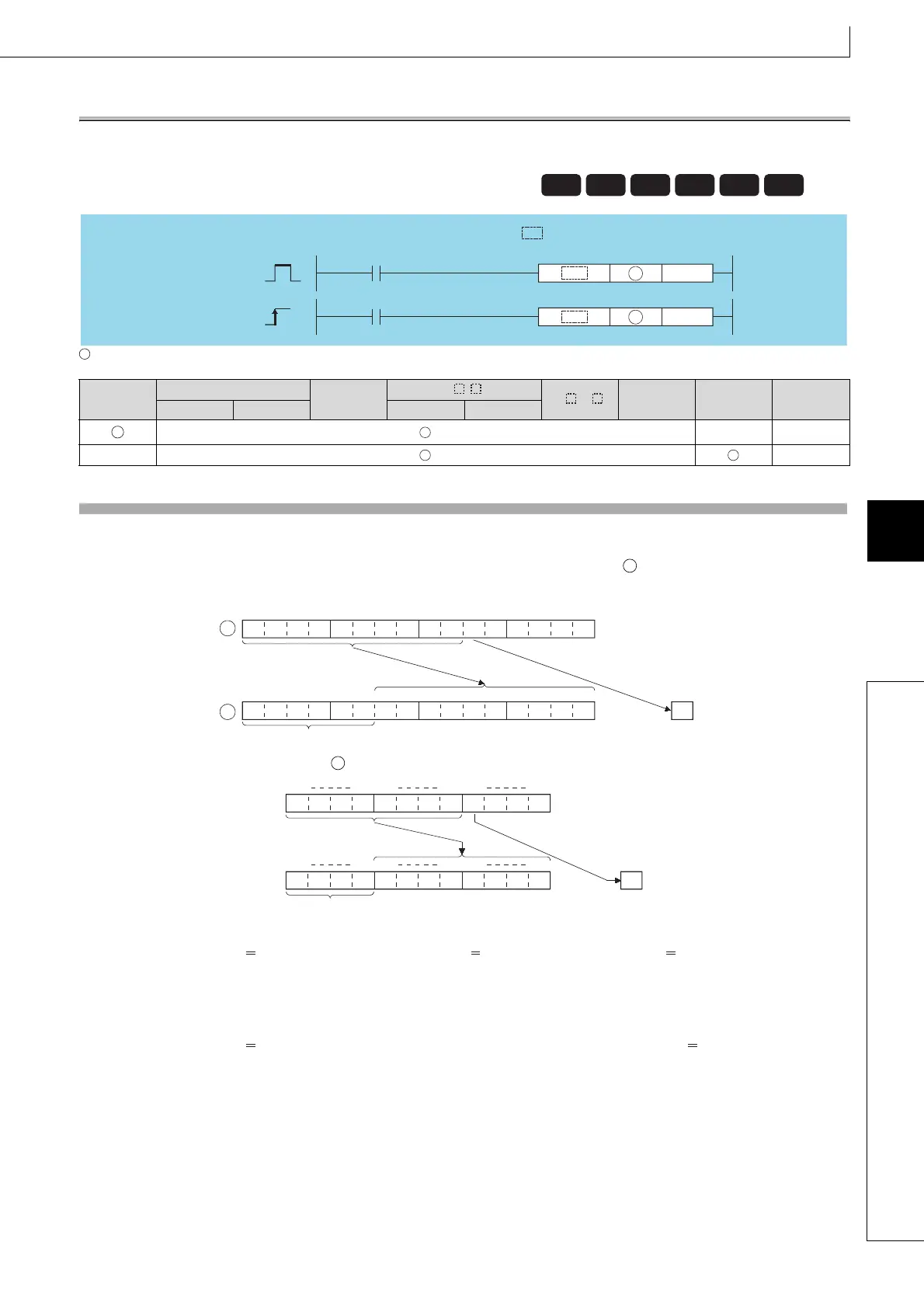
Details output instructions like OUT, SET, RST, PLS, PLF, FF, DELTA, and DELTAP for controlling outputs.
Explains instructions for shifting data, including SFR, SFRP, SFL, and SFLP.
Covers MC and MCR instructions for creating efficient ladder switching sequence programs.
Explains FEND and END instructions for program termination and sequence program end.
Lists other instructions like STOP, NOP, NOPLF, and PAGE, used for program control and stopping.
Explains instructions for comparing BIN 16-bit, BIN 32-bit, floating-point, and character string data.
Details arithmetic operations like addition, subtraction, multiplication, and division for BIN and floating-point data.
Covers instructions for converting data between BCD, BIN, floating-point, and ASCII formats.
Explains logical operations like AND, OR, XOR, and XNR for bit-wise data manipulation.
Covers instructions for rotating data bits, including ROR, ROL, DROR, and DRCL.
Details shift instructions like SFR, SFRP, SFL, and SFLP for moving data bits.
Explains instructions for bit manipulation such as BSET, BRST, TEST, and DTEST.
Covers instructions for data manipulation like search, sort, sum, average, decode, and encode.
Explains instructions for creating program structures like FOR/NEXT loops, CALL, FCALL, ECALL, EFCALL, and XCALL.
Details instructions for managing data tables, including FIFW, FIFR, FPOP, FDEL, FINS.
Covers instructions for accessing buffer memory, such as FROM, FROMP, DFRO, DFROP, TO, TOP, DTO, DTOP.
Explains instructions for displaying data, including PR, PRC, and LEDR.
Provides instructions for debugging and diagnosing failures, such as CHKST, CHK, CHKCIR, and CHKEND.
Covers instructions for processing character strings, including BINDA, HABIN, DABCD, STR, EVAL, etc.
Details special function instructions for mathematical operations like SIN, COS, TAN, ASIN, ACOS, ATAN, and their double precision counterparts.
Explains instructions for data control, including LIMIT, BAND, and ZONE operations for range and dead band control.
Details instructions for switching file registers, such as RSET, QDRSET, QCDSET.
Explains instructions for handling clock data, including DATERD, DATEWR, DATE+, DATE-, SECOND, HOUR, and TM instructions.
Covers instructions for refreshing network communication, specifically S.ZCOM and SP.ZCOM.
Explains instructions for reading and writing routing information, like S.RTREAD, SP.RTREAD, S.RTWRITE, and SP.RTWRITE.
Details instructions for writing data to the CPU shared memory, such as S.TO and TO.
Explains instructions for reading data from the CPU shared memory of other CPUs, such as FROM, FROMP, DFRO, DFROP.
Provides an overview of multiple CPU high-speed transmission dedicated instructions and their usage.
Explains the SP.CONTSW instruction for switching between control and standby systems.
Details the processing time for various instructions on different CPU modules.
Compares the performance of QCPU, LCPU with AnNCPU, AnACPU, and AnUCPU.
Provides example programs illustrating operations like nth power and nth root calculations.