Home
Motorola
Two-Way Radio
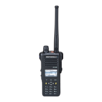
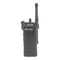
APX 2000
Motorola APX 2000 Detailed Service Manual
5
of 1
of 1 rating
1096 pages
Give review
Manual
Specs
To Next Page
To Next Page
To Previous Page
To Previous Page
Loading...
6-34
Troubleshootin
g Waveforms:
Rece
ive Baseband Signals
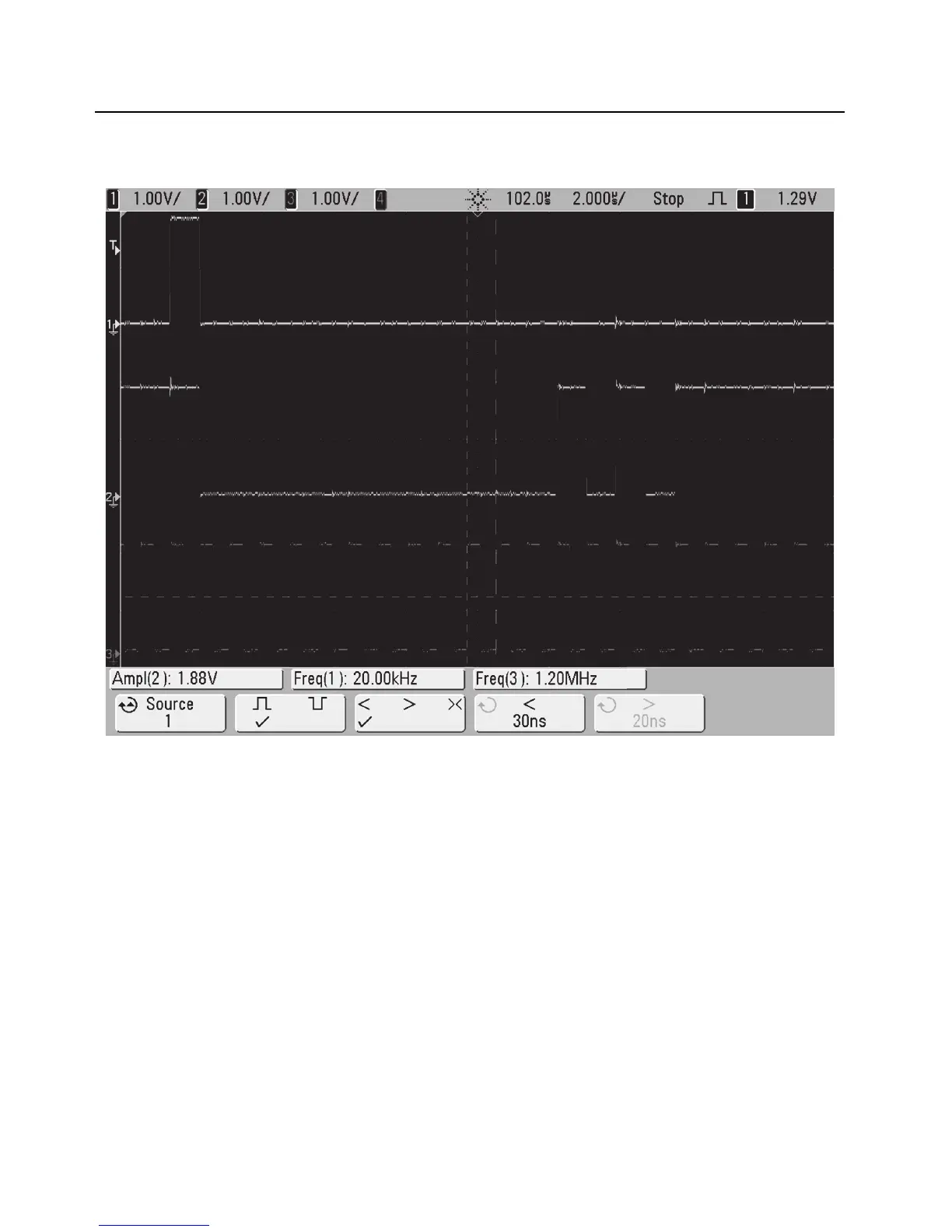
6.13
Receive Baseband Signals
T
race 1:
DIG_DA
T
A_SSI_RX_FS at R616.
T
race 2: DIG_DA
T
A
_SSI_RX_DOUT
A at R617.
T
race 3: CLK_SSI_RX at R618
.
Figure 6-33. Re
ceived Baseband W
aveforms
195
197
Table of Contents
Table of Contents
11
Default Chapter
2
Computer Software Copyrights
2
Disclaimer
2
Document Copyrights
2
Foreword
2
Manual Revisions
2
Product Safety and Rf Exposure Compliance
2
Trademarks
2
Document History
5
Commercial Warranty
7
Table of Contents
11
List of Tables
14
List of Figures
16
Chapter 1 Introduction
23
General
23
Notations Used in this Manual
24
Chapter 2 Radio Power
25
General
25
Table 2-1. IMPRES Batteries
25
DC Power Routing
26
Figure 2-1. DC Power Distribution
26
Chapter 3 Theory of Operation
27
Figure 3-1. APX 2000/ APX 4000/ APX 4000Li Overall Block Diagram
28
Figure 3-2. APX 1000 (900 Mhz) Overall Block Diagram
29
Main Board
30
Figure 3-3. Transceiver (VHF) Block Diagram (Power and Control Omitted)
30
Figure 3-4. Transceiver (UHF1/UHF2) Block Diagram (Power and Control Omitted)
31
Figure 3-5. Transceiver (700/800 Mhz) Block Diagram (Power and Control Omitted)
32
Table 3-1. Battery Connector J3
33
Figure 3-6. Transceiver (900 Mhz) Block Diagram (Power and Control Omitted)
33
Figure 3-7. Receiver Block Diagram (VHF)
34
Figure 3-8. Receiver Block Diagram (UHF1/UHF2)
35
Figure 3-9. Receiver Block Diagram (700/800 Mhz )
35
Figure 3-10. Receiver Block Diagram (900 Mhz )
35
Figure 3-11. Transmitter Block Diagram (VHF/UHF1/UHF2/900 Mhz)
37
Figure 3-12. Transmitter Block Diagram (700/800 Mhz)
38
Figure 3-13. Synthesizer Block Diagram (VHF)
42
Figure 3-14. Synthesizer Block Diagram (UHF1/UHF2)
43
Figure 3-15. Synthesizer Block Diagram (700/800 Mhz)
43
Figure 3-16. Synthesizer Block Diagram (900 Mhz)
44
Controller
49
Figure 3-17. Controller Interconnection Diagram
49
Figure 3-18. Controller Electrical Overview
51
Figure 3-19. Controller DC Block Diagram
52
Table 3-2. DC Supplies and Sources for Controller
53
Table 3-3. Mako's LDO and Supplies
54
Figure 3-20. V_SW_1.4 Switched Power Supply
55
Table 3-4. Pulse Switching Combination
56
Figure 3-21. 5V Switched Power Supply
56
Figure 3-22. Power-Up Timing Regulators
57
Figure 3-23. Controller Clock Architecture
58
Table 3-5. Controller Clock Distribution
59
Figure 3-24. Overview of OMAP Interconnection with Controller Peripherals
60
Figure 3-25. OMAP Memory Interface
61
Figure 3-26. RX/ TX SSI Configuration
62
Figure 3-27. Audio SSI Configuration
63
Figure 3-28. SPI and I2C Configuration
64
Figure 3-29. CPLD Block Diagram
65
Figure 3-30. Audio TX Path Block Diagram
66
Figure 3-31. RX Audio Path Block Diagram
67
Figure 3-32. Control Top Block Diagram (APX 2000/ APX 4000/ APX 4000Li/ APX 1000 (900 Mhz))
68
Figure 3-33. Control Top Block Diagram (APX 2000/ APX 4000 (Two Knobs))
69
Figure 3-34. Display Circuit Detail Overview Block Diagram
70
Table 3-6. Color Schemes
71
Figure 3-35. Lighting Controller Overview
72
Table 3-7. Key Map Matrix
73
Figure 3-36. Keypad Interface Outline
73
Figure 3-37. GCAI Signal Configuration
74
Table 3-8. P1 Pin Assignment
75
Figure 3-38. GCAI Connector
75
Table 3-9. GCAI Connector Pin Assignment
76
Figure 3-39. APX 2000/ APX 4000 Encryption Architecture
77
Table 3-10. Secure Keypad KIT Numbers
78
Global Positioning Sytem (GPS)
79
Table 3-11. Power and I/O Pins for NL5500
80
Figure 3-40. GPS Block Diagram
80
Accelerometer
81
Table 3-12. SPI Interface
81
Figure 3-41. Accelerometer Block Diagram
81
Table 3-13. Register Address Map
82
Bluetooth
83
Figure 3-42. Relation of Bluetooth & LF Antenna Assembly to Main & Keypad Boards
83
Figure 3-43. Bluetooth Connection Flowchart
84
Figure 3-44. Bluetooth/Controller Interface with Clock Sources
85
Figure 3-45. Bluetooth Functional Block Diagram
85
Figure 3-46. Bluetooth Low-Frequency Circuit Block Diagram
86
Figure 3-47. Bluetooth Low-Frequency Pairing Data Path
86
Figure 3-48. Detailed Low-Frequency Transmit/Receive Paths
87
Figure 3-49. Chip Power-Up/Power-Down Sequence (Exernal Input/Output Shown)
87
Figure 3-50. Current Distribution Tree for Bluetooth Circuitry
88
Table 3-14. Bluetooth Host Processor UART I/O
89
Table 3-15. SPI I/O
90
Figure 3-51. Bluetooth LF UART Connection Block Diagram
90
Table 3-16. USB I/O
91
Figure 3-52. Bluetooth USB Interface to Main Board
91
Table 3-17. GPIO I/O
92
Chapter 4 Troubleshooting Procedures
93
Handling Precautions
93
Recommended Service Tools
94
Table 4-1. Recommended Service Tools
94
Standard Bias Table
95
Table 4-2. Standard Operating Bias - DC Voltages
95
Table 4-3. Standard Operating Bias - Clock Sources
95
Power-Up Self-Check Errors
96
Table 4-4. Power-Up Self-Check Error Codes
96
Power-Up Self-Check Diagnostics and Repair (Not for Field Use)
97
Table 4-5. Power-Up Self-Check Diagnostic Actions
97
Chapter 5 Troubleshooting Charts
99
List of Troubleshooting Charts
99
Table 5-1. Troubleshooting Charts
99
Main Troubleshooting Flowchart
101
Power-Up Failure
102
DC Supply Failure
113
Main Display Failure
120
Volume/Channel Error
121
Volume Set Error (APX 2000/ APX 4000 (Two Knobs))
122
Channel Select Error (APX 2000/ APX 4000 (Two Knobs))
123
Keypad Error
124
5.10 Side Button Error
125
5.11 RX Audio Error
126
5.12 TX Audio Error
128
5.13 Keyload/Secure Hardware/Memory
130
RX RF Failure
132
5.15 FGU Failure
143
VCO Failure
144
5.17 GPS Failure
150
Bluetooth Failure
152
PA Failure
157
Chapter 6 Troubleshooting Waveforms
163
List of Waveforms
163
Table 6-1. List of Waveforms
163
Clocks
164
Figure 6-1. 32 Khz Clock Waveform
164
Figure 6-2. 4 Mhz Clock Waveform
165
Figure 6-3. 12 Mhz Clock Waveform
166
Figure 6-4. 16.8 Mhz Clock Waveform
167
Figure 6-5. 24 Mhz Clock Waveform
168
Audio SSI
169
Figure 6-6. Audio SSI - Red Tx Waveform
169
Figure 6-7. Audio SSI - Red Rx Waveform
170
Figure 6-8. Audio SSI - Sync. Waveform
171
Figure 6-9. Audio SSI - BCLK. Waveform
172
Rx Ssi
173
Figure 6-10. RX SSI - CLK. Waveform
173
Figure 6-11. RX SSI - da Waveform
174
Figure 6-12. RX SSI - Fsync. Waveform
175
Tx Ssi
176
Figure 6-13. TX SSI - TX CLK. Waveform
176
Figure 6-14. TX SSI - da Waveform
177
Figure 6-15. TX SSI - Fsync. Waveform
178
Spi
179
Figure 6-16. SPI - CLK Waveform
179
Figure 6-17. CS Waveform
180
I2C Bus
181
Figure 6-18. I2C Bus - SCA Waveform
181
Figure 6-19. I2C Bus - SCA 5V Waveform
182
Figure 6-20. I2C Bus - SDA Waveform
183
One Wire
184
Figure 6-21. 1-Wire Waveform
184
Gcai
185
Figure 6-22. GCAI - GPIO0 Waveform
185
Figure 6-23. GCAI - GPIO4 Waveform
186
6.10 Usb
187
Figure 6-24. USB - D- Waveform
187
Figure 6-25. USB - D+ Waveform
188
6.11 Sdram
189
Figure 6-26. SDRAM - CLK Waveform
189
Figure 6-27. SDRAM - CLKX Waveform
190
6.12 Flash Control
191
Figure 6-28. FLASH CONTROL - ADV Waveform
191
Figure 6-29. FLASH CONTROL - CS3 Waveform
192
Figure 6-30. FLASH CONTROL - OE Waveform
193
Figure 6-31. FLASH CONTROL - RDY Waveform
194
Figure 6-32. FLASH CONTROL - WE Waveform
195
6.13 Receive Baseband Signals
196
Figure 6-33. Received Baseband Waveforms
196
6.14 Gps
197
Figure 6-34. GPS TCXO Waveforms
197
Figure 6-35. GPS RTC Waveforms
198
Figure 6-36. GPS UART DATA Waveforms
199
6.15 Bluetooth Troubleshooting Waveforms
200
Table 6-2. Bluetooth Command to TX
200
Table 6-3. Bluetooth Command to RX
201
Table 6-4. Low Frequency Command to TX
201
Table 6-5. Low Frequency Command to RX
201
Table 6-6. Bluetooth Test Points
202
Figure 6-37. Startup Waveforms - Vmax of TP16
203
Figure 6-38. Startup - Timing Difference of TP9 to TP16
204
Figure 6-39. Startup - Timing Difference of TP5 to TP16 and Voltage Statistics
205
Figure 6-40. Startup - Timing Difference of TP4 to TP16 and Time Statistics
206
Figure 6-41. Startup - Timing Difference of TP4 to TP5 and Time Statistics
207
Figure 6-42. Startup - Vmax of TP5 and Time Statistics
208
Figure 6-43. Startup - Vmax of TP4 and Time Statistics
209
Figure 6-44. Startup - Vmax of TP5 and Voltage Statistics
210
Figure 6-45. Startup - Vmax of TP9 and Voltage Statistics
211
Figure 6-46. Startup - Vmax of TP10 and Time Statistics
212
Figure 6-47. Startup - Vmax of TP16 and Voltage Statistics
213
Figure 6-48. Startup - Vmax of TP13 and Voltage Statistics
214
Figure 6-49. Startup - Vmax of TP11 and Voltage Statistics
215
Figure 6-50. Startup - Timing Difference of TP13 to TP16 and Time Statistics
216
Figure 6-51. Startup - Timing Difference of TP10 to TP13 and Time Statistics
217
Figure 6-52. Startup - Timing Difference of TP11 to TP13 and Time Statistics
218
Figure 6-53. Bluetooth CW on Spectrum Analyzer
219
6.16 Bluetooth Steady-State
220
Figure 6-54. Keypad Board - USB D+ Vmax and Packet Timing with Statistics
220
Figure 6-55. Keypad Board - USB D- Vmax and Packet Timing with Statistics
221
Figure 6-56. Keypad Board - VSW_3.6 Voltage Statistics
222
Figure 6-57. Keypad Board - 32 Khz Clock Vmax with Statistics
223
Figure 6-58. Keypad Board Waveforms - LF Coil When TX and RX
224
6.17 LF CW on Spectrum Analyzer
225
Figure 6-59. LF CW on Spectrum Analyzer
225
Chapter 7 Troubleshooting Tables
227
List of Board and IC Signals
227
Table 7-2. Mainboard to Back Kit Flex Connector Interface Pin-Out
228
Table 7-3. Main Back Kit Flex Connector to Main Board Connector Interface Pin-Out
231
Table 7-4. Main Back Kit Flex Connector to Keypad Board Connector Interface Pin-Out
234
Table 7-5. Keypad Board Connector to Mainboard Interface Pin-Out
237
Table 7-6. Keypad Board Connector to Front Kit Flex Interface Pin-Out
240
Table 7-7. Front Kit Connector Interface Pin-Out
242
Table 7-8. GCAI Flex Connector Interface Pin-Out
247
Table 7-9. PTT Flex Connector Interface Pin-Out
249
Table 7-10. Mainboard to Back Kit Flex Connector Interface Pin-Out
250
Table 7-11. Main Back Kit Flex Connector to Main Board Connector Interface Pin-Out
252
Table 7-12. Main Back Kit Flex Connector to Keypad Board Connector Interface Pin-Out
255
Table 7-13. Keypad Board Connector to Mainboard Interface Pin-Out
258
Table 7-14. Keypad Board Connector to Front Kit Flex Interface Pin-Out
261
Table 7-15. Front Kit Connector Interface Pin-Out
264
Table 7-16. GCAI Flex Connector Interface Pin-Out
269
Table 7-17. PTT Flex Connector Interface Pin-Out
271
Table 7-18. Overall GPIO Pin Functions
272
Table 7-19. Primary IC Reference Designator
280
Chapter 8 Schematics, Boards Overlays, and Parts Lists
281
List of Transceiver Schematics and Board Overlays
281
Table 8-1. List of Transceiver Schematics and Board Overlays
281
Figure 8-1. Transceiver (RF) Mainboard Overall Schematic (84012320001)
281
Figure 8-36. Transceiver (RF) Board Layout - Top Side (84012320001)
281
Figure 8-37. Transceiver (RF) Board Layout - Bottom Side (84012320001)
281
Figure 8-40. Transceiver (RF) Mainboard Overall Schematic (84012313002)
281
Figure 8-75. Transceiver (RF) Board Layout - Top Side (84012313002)
282
Figure 8-76. Transceiver (RF) Board Layout - Bottom Side (84012313002)
282
Figure 8-79. Transceiver (RF) Mainboard Overall Schematic (84012432001)
282
Figure 8-114.Transceiver (RF) Board Layout - Top Side (84012432001)
282
Figure 8-115.Transceiver (RF) Board Layout - Bottom Side (84012432001)
282
Figure 8-118.Transceiver (RF) Board Overall Schematic (84012266001)
282
Figure 8-152.Transceiver (RF) Board Layout - Top Side (84012266001)
282
Figure 8-153.Transceiver (RF) Board Layout - Bottom Side (84012266001)
282
Transceiver (RF) Boards: VHF (84012320001 / PC000352A01)
285
Figure 8-4. Controller Mainboard Circuit
288
Figure 8-5. ANTSWI Circuit
289
Figure 8-6. TX HF Circuit
290
Figure 8-7. Power Amplifier (PA) Circuit
291
Figure 8-8. Automatic Level Control Circuit
292
Figure 8-9. Receiver Front End Circuit
293
Figure 8-12. Receiver VCO Circuit
296
Figure 8-13. Transmitter VCO Circuit
297
Figure 8-14. DC Circuit
298
Figure 8-15. RF Interconnects Circuit
299
Figure 8-16. CPLD Circuit
300
Figure 8-17. OMAP User Interface Circuit
301
Figure 8-18. Memory Interface Circuit (84012320001)
302
Figure 8-19. Memory Interface Circuit (PC000352A01)
303
Figure 8-20. Audio Circuit (84012320001)
304
Figure 8-21. Audio Circuit (PC000352A01)
305
Figure 8-22. MAKO/DC Distribution Circuit (84012320001)
306
Figure 8-23. MAKO/DC Distribution Circuit (PC000352A01)
307
Figure 8-24. Serial Interface Circuit
308
Figure 8-25. GPS Bluetooth Circuit
309
Figure 8-26. Controller Circuit (84012320001)
310
Figure 8-27. Controller Circuit (PC000352A01)
311
Figure 8-28. Display/Keypad Lighting Control Circuit (84012320001)
312
Figure 8-29. Display/Keypad Lighting Control Circuit (PC000352A01)
313
Figure 8-30. LCD and Keypad Connector Circuit (84012320001)
314
Figure 8-31. LCD and Keypad Connector Circuit (PC000352A01)
315
Figure 8-32. GCAI MACE BT Interconnect Circuit (84012320001)
316
Figure 8-33. GCAI MACE BT Interconnect Circuit (PC000352A01)
317
Figure 8-38. Transceiver (RF) Board Layout - Top Side (PC000352A01)
322
Figure 8-39. Transceiver (RF) Board Layout - Bottom Side (PC000352A01)
323
Transceiver (RF) Boards: UHF1 (84012313002 / PC000353A01)
363
Figure 8-43. Controller Mainboard Circuit
366
Figure 8-44. DC Circuit
367
Figure 8-45. Receiver Back End Circuit
368
Figure 8-46. Receiver Front End Circuit
369
Figure 8-47. ANTSWI Circuit
370
Figure 8-48. Automatic Level Control Circuit
371
Figure 8-49. Receiver Back End Circuit
372
Figure 8-52. Power Amplifiercircuit
375
Figure 8-53. Transmitter HF Circuit
376
Figure 8-54. Receiver VCO Circuit
377
Figure 8-55. Transmitter VCO Circuit
378
Figure 8-56. CPLD Circuit
379
Figure 8-57. OMAP User Interface Circuit
380
Figure 8-58. Memory Interface Circuit (84012313002)
381
Figure 8-59. Memory Interface Circuit (PC000353A01)
382
Figure 8-60. Audio Circuit (84012313002)
383
Figure 8-61. Audio Circuit (PC000353A01)
384
Figure 8-62. MAKO/DC Distribution Circuit (84012313002)
385
Figure 8-63. MAKO/DC Distribution Circuit (PC000353A01)
386
Figure 8-64. Serial Interface Circuit
387
Figure 8-65. RF Interconnects Circuit
388
Figure 8-66. Controller Circuit (84012313002)
389
Figure 8-67. Controller Circuit (PC000353A01)
390
Figure 8-68. Display/Keypad Lighting Control Circuit (84012313002)
391
Figure 8-69. Display/Keypad Lighting Control Circuit (PC000353A01)
392
Figure 8-70. LCD and Keypad Connector Circuit (84012313002)
393
Figure 8-71. LCD and Keypad Connector Circuit (PC000353A01)
394
Figure 8-72. GCAI MACE BT Interconnect Circuit (84012313002)
395
Figure 8-73. GCAI MACE BT Interconnect Circuit (PC000353A01)
396
Figure 8-74. GPS Bluetooth Circuit
397
Figure 8-77. Transceiver (RF) Board Layout - Top Side (PC000353A01)
400
Figure 8-78. Transceiver (RF) Board Layout - Bottom Side (PC000353A01)
401
Transceiver (RF) Boards: UHF2 (84012432001 / PC000354A01)
441
Figure 8-82. Controller Mainboard Circuit
444
Figure 8-83. DC Circuit
445
Figure 8-84. Transmitter HF Circuit
446
Figure 8-85. Power Amplifier Circuit
447
Figure 8-86. Automatic Level Control Circuit
448
Figure 8-87. Receiver Front End Circuit
449
Figure 8-90. Receiver VCO Circuit
452
Figure 8-91. Transmitter VCO Circuit
453
Figure 8-94. DC Circuit
456
Figure 8-95. RF Interconnects Circuit
457
Figure 8-96. CPLD Circuit
458
Figure 8-97. OMAP User Interface Circuit
459
Figure 8-98. Memory Interface Circuit (84012432001)
460
Figure 8-99. Memory Interface Circuit (PC000354A01)
461
Figure 8-100.Audio Circuit (84012432001)
462
Figure 8-101.Audio Circuit (PC000354A01)
463
Figure 8-102.MAKO/DC Distribution Circuit (84012432001)
464
Figure 8-103.MAKO/DC Distribution Circuit (PC000354A01)
465
Figure 8-104.Serial Interface Circuit
466
Figure 8-105.GPS Bluetooth Circuit
467
Figure 8-106.Controller Circuit (84012432001)
468
Figure 8-107.Controller Circuit (PC000354A01)
469
Figure 8-108.Display/Keypad Lighting Control Circuit (84012432001)
470
Figure 8-109.Display/Keypad Lighting Control Circuit (PC000354A01)
471
Figure 8-110.LCD and Keypad Connector Circuit (84012432001)
472
Figure 8-111.LCD and Keypad Connector Circuit (PC000354A01)
473
Figure 8-112.GCAI MACE BT Interconnect Circuit (84012432001)
474
Figure 8-113.GCAI MACE BT Interconnect Circuit (PC000354A01)
475
Figure 8-116.Transceiver (RF) Board Layout - Top Side (PC000354A01)
478
Figure 8-117.Transceiver (RF) Board Layout - Bottom Side (PC000354A01)
479
Transceiver (RF) Boards: 700 - 800 Mhz (84012266001 / PC000351A01)
519
Figure 8-121.Controller Mainboard Circuit
522
Figure 8-122.DC Circuit
523
Figure 8-123.Receiver Back End Circuit
524
Figure 8-124.Receiver Front End Circuit
525
Figure 8-125.ANTSWI Circuit
526
Figure 8-126.Automatic Level Control Circuit
527
Figure 8-127.Receiver Back End Circuit
528
Figure 8-130.Power Amplifiercircuit
531
Figure 8-131.Transmitter HF Circuit
532
Figure 8-132.VCO Circuit
533
Figure 8-133.CPLD Circuit
534
Figure 8-134.OMAP User Interface Circuit
535
Figure 8-135.Memory Interface Circuit (84012266001)
536
Figure 8-136.Memory Interface Circuit (PC000351A01)
537
Figure 8-137.Audio Circuit (84012266001)
538
Figure 8-138.Audio Circuit (PC000351A01)
539
Figure 8-139.MAKO/DC Distribution Circuit (84012266001)
540
Figure 8-140.MAKO/DC Distribution Circuit (PC000351A01)
541
Figure 8-141.Serial Interface Circuit
542
Figure 8-142.RF Interconnects Circuit
543
Figure 8-143.Controller Circuit (84012266001)
544
Figure 8-144.Controller Circuit (PC000351A01)
545
Figure 8-145.Display/Keypad Lighting Control Circuit (84012266001)
546
Figure 8-146.Display/Keypad Lighting Control Circuit (PC000351A01)
547
Figure 8-147.LCD and Keypad Connector Circuit (84012266001)
548
Figure 8-148.LCD and Keypad Connector Circuit (PC000351A01)
549
Figure 8-149.GCAI MACE BT Interconnect Circuit (84012266001)
550
Figure 8-150.GCAI MACE BT Interconnect Circuit (PC000351A01)
551
Figure 8-151.GPS Bluetooth Circuit
552
Figure 8-154.Transceiver (RF) Board Layout - Top Side(PC000351A01)
555
Figure 8-155.Transceiver (RF) Board Layout - Bottom Side (PC000351A01)
556
Transceiver (RF) Boards: 900 Mhz (84012478001)
595
Figure 8-156.Transceiver (RF) Board Overall Schematic
595
Figure 8-157.Controller Mainboard Circuit
596
Figure 8-158.DC Circuit
597
Figure 8-159.Receiver Back End Circuit
598
Figure 8-160.Receiver Front End Circuit
599
Figure 8-161.ANTSWI Circuit
600
Figure 8-162.Automatic Level Control Circuit
601
Figure 8-163.Receiver Back End Circuit
602
Figure 8-166.Power Amplifier Circuit
605
Figure 8-167.Transmitter HF Circuit
606
Figure 8-168.Receive and Transmit VCO Circuit
607
Figure 8-169.CPLD Circuit
608
Figure 8-170.OMAP User Interface Circuit
609
Figure 8-171.Memory Interface Circuit
610
Figure 8-172.Audio Circuit
611
Figure 8-173.MAKO/DC Distribution Circuit
612
Figure 8-174.Serial Interface Circuit
613
Figure 8-175.RF Interconnects Circuit
614
Figure 8-176.Controller Circuit
615
Figure 8-177.Display/Keypad Lighting Control Circuit
616
Figure 8-178.LCD and Keypad Connector Circuit
617
Figure 8-179.GCAI MACE BT Interconnect Circuit
618
Figure 8-180.GPS Bluetooth Circuit
619
Figure 8-181.Transceiver (RF) Board Layout - Top Side
620
Figure 8-182.Transceiver (RF) Board Layout - Bottom Side
621
Keypad Board (84012282001)
639
Figure 8-183.Keypad Board Overall Circuit Schematic (Basic)
639
Figure 8-184.Keypad Matrix Circuit (Basic)
640
Figure 8-185.Keypad Board Overall Circuit Schematic (Expanded)
641
Figure 8-186.Keypad Matrix Circuit (Expanded)
642
Figure 8-187.GPS Bluetooth Circuit
643
Figure 8-188.MACE Circuit
644
Figure 8-189.Keypad Board Layout - Top Side
645
Figure 8-190.Keypad Board Layout - Bottom Side
646
Keypad Lite Board (84012559002)
661
Figure 8-191.Keypad Lite Board Overall Circuit Schematic
661
Figure 8-192.Keypad Lite Matrix Circuit
662
Figure 8-193.Keypad Lite Board Layout - Top Side
663
Figure 8-194.Keypad Lite Board Layout - Bottom Side
664
Keypad Board (APX 2000/ APX 4000 (Two Knobs)) (PC000356A02 (Model 2) / PC000356A01 (Model 3))
667
Figure 8-195.Keypad Board Overall Circuit Schematic (Expanded)
667
Figure 8-196.Keypad Matrix Circuit (Expanded)
668
Figure 8-197.GPS Bluetooth Circuit
669
Figure 8-198.MACE Circuit
670
Figure 8-199.Keypad Board Layout - Top Side
671
Figure 8-200.Keypad Board Layout - Bottom Side
672
Glossary
685
Table of Contents
691
Appendix A EMEA Warranty, Service and Technical Support
693
List of Tables
695
List of Figures
696
Chapter 1 Introduction
701
General
701
Notations Used in this Manual
702
Chapter 2 Radio Power
703
General
703
DC Power Routing
704
Chapter 3 Theory of Operation
705
Main Board
707
Controller
725
Chapter 4 Troubleshooting Procedures
751
Handling Precautions
751
Recommended Service Tools
752
Standard Bias Table
753
Power-Up Self-Check Errors
754
Power-Up Self-Check Diagnostics and Repair (Not for Field Use)
755
Chapter 5 Troubleshooting Charts
757
List of Troubleshooting Charts
757
Main Troubleshooting Flowchart
759
Power-Up Failure
760
DC Supply Failure
771
Main Display Failure
778
Volume/Channel Error
779
Keypad Error
780
Side Button Error
781
RX Audio Error
782
5.10 TX Audio Error
784
RX RF Failure
786
5.12 FGU Failure
797
VCO Failure
798
PA Failure
802
Chapter 6 Troubleshooting Waveforms
807
List of Waveforms
807
Clocks
808
Audio SSI
813
Rx Ssi
817
Tx Ssi
820
Spi
823
I2C Bus
825
One Wire
828
Gcai
829
6.10 Usb
831
6.11 Sdram
833
6.12 Flash Control
835
6.13 Receive Baseband Signals
840
Chapter 7 Troubleshooting Tables
841
List of Board and IC Signals
841
Chapter 8 Schematics, Boards Overlays, and Parts Lists
873
List of Transceiver Schematics and Board Overlays
873
A.1 Warranty and Service Support
1065
A.2 European Radio Support Centre (ERSC)
1066
A.4 Technical Support
1067
B.2 Replacement Parts Ordering
1071
C.2 Replacement Parts Ordering
1075
C.3 Motorola Service Centers
1076
Technical Support
1077
D.3 Motorola Service Centers
1078
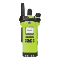
Other manuals for Motorola APX 2000
User Guide
206 pages
Basic Service Manual
526 pages
Quick Reference Guide
46 pages
5
Based on 1 rating
Ask a question
Give review
Questions and Answers:
Need help?
Do you have a question about the Motorola APX 2000 and is the answer not in the manual?
Ask a question
Motorola APX 2000 Specifications
General
Brand
Motorola
Model
APX 2000
Category
Two-Way Radio
Language
English
Related product manuals
Motorola APX 2500
201 pages
Motorola APX 1000i 2
126 pages
Motorola APX 6000XE 2
48 pages
Motorola APX 6000XE 2.5
82 pages
Motorola APX 6000
200 pages
Motorola APX 4500
201 pages
Motorola APX 6500
52 pages
Motorola APX 8500
273 pages
Motorola APX 7500
70 pages
Motorola APX 5000
318 pages
Motorola APX 8000
161 pages
Motorola APX 7000
213 pages