xii List of Figures
List of Figures
Figure 2-1. DC Power Distribution........................................................................................................... 2-2
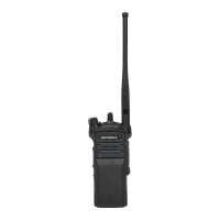
Figure 3-1. APX 1000 Overall Block Diagram ......................................................................................... 3-2
Figure 3-2. Transceiver (VHF) Block Diagram (Power and Control Omitted).......................................... 3-3
Figure 3-3. Transceiver (UHF1) Block Diagram (Power and Control Omitted) ....................................... 3-4
Figure 3-4. Transceiver (UHF2) Block Diagram (Power and Control Omitted) ....................................... 3-5
Figure 3-5. Transceiver (700/800 MHz) Block Diagram (Power and Control Omitted) ........................... 3-6
Figure 3-6. Receiver Block Diagram (VHF) ............................................................................................. 3-8
Figure 3-7. Receiver Block Diagram (UHF1/UHF2 ) ............................................................................... 3-8
Figure 3-8. Receiver Block Diagram (700/800 MHz ).............................................................................. 3-9
Figure 3-9. Transmitter Block Diagram.................................................................................................. 3-10
Figure 3-10. Synthesizer Block Diagram (VHF) ...................................................................................... 3-14
Figure 3-11. Synthesizer Block Diagram (UHF1/UHF2).......................................................................... 3-15
Figure 3-12. Synthesizer Block Diagram (700/800 MHz) ........................................................................ 3-15
Figure 3-13. Controller Interconnection Diagram .................................................................................... 3-21
Figure 3-14. Controller Electrical Overview ............................................................................................. 3-23
Figure 3-15. Controller DC Block Diagram .............................................................................................. 3-24
Figure 3-16. V_SW_1.4 Switched Power Supply .................................................................................... 3-27
Figure 3-17. 5V Switched Power Supply ................................................................................................. 3-28
Figure 3-18. Power-up Timing Regulators............................................................................................... 3-29
Figure 3-19. Controller Clock Architecture .............................................................................................. 3-30
Figure 3-20. Overview of OMAP Interconnection with Controller Peripherals......................................... 3-31
Figure 3-21. OMAP Memory Interface..................................................................................................... 3-32
Figure 3-22. RX / TX SSI Configuration .................................................................................................. 3-33
Figure 3-23. Audio SSI Configuration...................................................................................................... 3-34
Figure 3-24. SPI and I2C Configuration .................................................................................................. 3-35
Figure 3-25. CPLD Block Diagram .......................................................................................................... 3-36
Figure 3-26. Audio TX Path Block Diagram............................................................................................. 3-37
Figure 3-27. RX Audio Path Block Diagram ............................................................................................ 3-38
Figure 3-28. Control Top Block Diagram ................................................................................................. 3-39
Figure 3-29. Display Circuit Detail Overview Block Diagram................................................................... 3-40
Figure 3-30. Lighting Controller Overview ............................................................................................... 3-42
Figure 3-31. Keypad Interface Outline..................................................................................................... 3-43
Figure 3-32. GCAI Signal Configuration .................................................................................................. 3-44
Figure 3-33. GCAI Connector.................................................................................................................. 3-45
Figure 6-1. 32 kHz Clock Waveform........................................................................................................ 6-2
Figure 6-2. 4 MHz Clock Waveform ........................................................................................................ 6-3
Figure 6-3. 12 MHz Clock Waveform ...................................................................................................... 6-4
Figure 6-4. 16.8 MHz Clock Waveform ................................................................................................... 6-5
Figure 6-5. 24 MHz Clock Waveform ...................................................................................................... 6-6
Figure 6-6. Audio SSI – Red Tx Waveform ............................................................................................. 6-7
Figure 6-7. Audio SSI – Red Rx Waveform............................................................................................. 6-8
Figure 6-8. Audio SSI – Sync. Waveform................................................................................................ 6-9
Figure 6-9. Audio SSI – BCLK. Waveform ............................................................................................ 6-10
Figure 6-10. RX SSI – CLK. Waveform ................................................................................................... 6-11
Figure 6-11. RX SSI – DA Waveform ...................................................................................................... 6-12
Figure 6-12. RX SSI – FSync. Waveform................................................................................................ 6-13
Figure 6-13. TX SSI – TX CLK. Waveform.............................................................................................. 6-14
Figure 6-14. TX SSI – DA Waveform ...................................................................................................... 6-15
Figure 6-15. TX SSI – FSync. Waveform ................................................................................................ 6-16
Figure 6-16. SPI – CLK Waveform .......................................................................................................... 6-17
 Loading...