Theory of Operation: Main Board 3-7
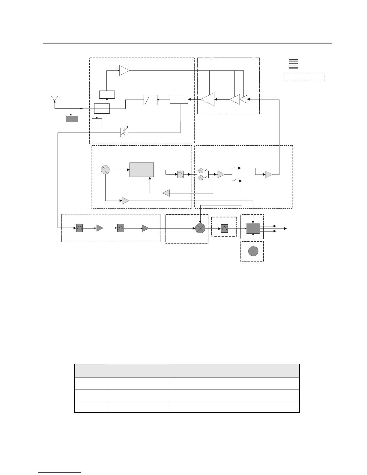
Figure 3-6. Transceiver (900 MHz) Block Diagram (Power and Control Omitted)
3.1.1 Interconnections
This section describes the various interconnections for the main board.
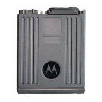
3.1.1.1 Battery Connector M101
Battery connector M101 solders to the transceiver printed circuit board. The connector has 5 gold
plated contacts that mate with the battery, two contacts for positive, two for negative and one for the
Dig_Battery_Data. Signal descriptions are in Table 3-1.
Table 3-1. Battery Connector J3
Pin No. Signal Description
1 DC_BATT Battery positive terminal, nominally 7.5 Vdc
2 Dig_Battery_Data Battery status, from battery to controller
3 Ground Battery negative terminal, tied to PCB ground
FGU
Transmitter
Receiver
2nd
LO
Digital
RF Atten
Antenna Switch
coupler
Rev
Power
Detector
Log
Amp
FET
TRIDENT IC
LOOP
FILTER
PRESCALAR
BUFFER
RX SSI Data
16.8MHz
BUFFER
PRE
BUFFER
TX LO
TX
BUFFER
TX
RX
*
16.8MHz
RX SSI Clock
RX SSI Frame Sync
Indicates Sub-shield
Harmonic
Filter
Driver
Amplifier
*
Abacus
IF Filter
15dB Step Attn
RX VCO
TX VCO
900
LNA
900
Mixer
LNA
GPS
 Loading...