Basic Theory of Operation: Analog Mode of Operation 3-3
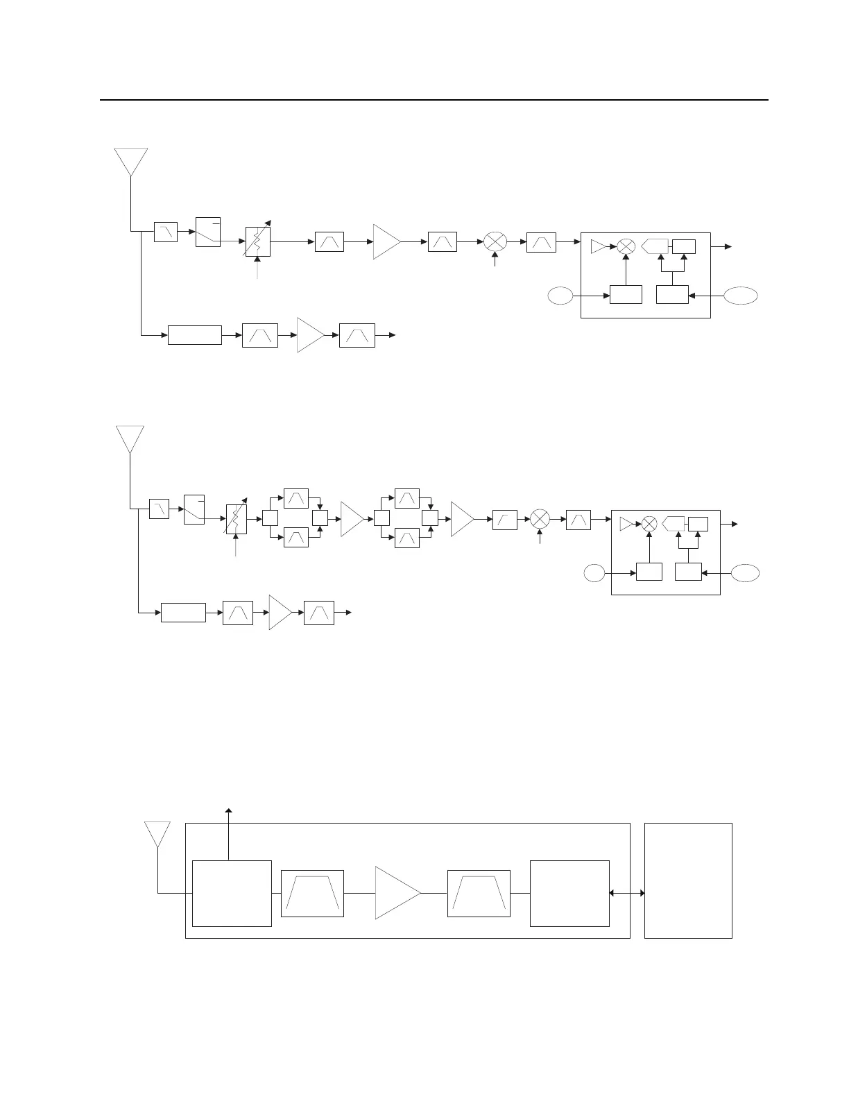
Figure 3-4. Receiver Block Diagram (VHF)
Figure 3-5. Receiver Block Diagram (700/800 MHz)
3.2.1.1 GPS
The GPS signal is tapped at the antenna port via a series resonant network (diplexer) which provides
a very low capacitive load to the transceiver. The diplexer circuitry provides rejection to radio band
signals up to ~1GHz which serves as isolation between the radio RF and GPS signal paths. The
GPS signal is filtered though a GPS SAW filter - LNA – Saw filter chain before going into the TI GPS
IC for processing.
Figure 3-6. GPS Diagram
15 dB Step
Attenuator
Antenna
Switch
DIG_CTRL_ATTH
VHF
Rx LO
IF Filter
To GPS
Diplexer
VHF
SSI
18Mhz
CLK
Abacus III
ABACUS III
Dec.
Filter
ΣΔ ADC
2nd
LO
LO CLK
15 dB Step
Attenuator
Antenna
Switch
SW
DIG_CTRL_ATTH
700
800
700
800
Rx LO
IF Filter
To GPS
Diplexer
SW SW SW
SSI
18Mhz
CLK
Abacus III
ABACUS III
Dec.
Filter
ΣΔ ADC
2nd
LO
LO CLK
To Radio transceiver path
GPS IC
GPS Receiver Circuit
ntenna
OMAP
Processor
Diplexer
 Loading...