21
21-15
ELECTRICAL CHARACTERISTICS
32180 Group User's Manual (Rev.1.0)
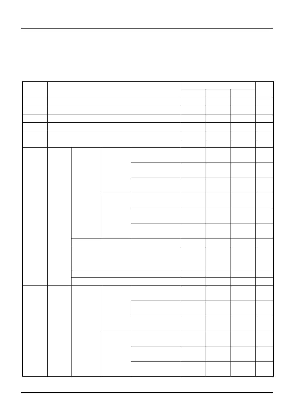
Symbol Parameter Rated Value Unit
MIN TYP MAX
VCCE Main Power Supply (Note 1) 3.0 3.3 3.6 V
OSC-VCC Clock Power Supply (Note 1) 3.0 VCCE 3.6 V
VCC-BUS Bus Power Supply (Note 1) 3.0 VCCE 3.6 V
VDDE RAM Power Supply (Note 1) 3.0 VCCE 3.6 V
AVCC Analog Power Supply (Note 1) 3.0 VCCE 3.6 V
VREF Reference Voltage Input (Note 1) 3.0 VCCE 3.6 V
VIH Input High When When Threshold selection 0.5VCCE VCCE V
Voltage threshold CMOS input : 0.35 VCCE
(Note 4) switching is selected Threshold selection 0.65VCCE VCCE V
function is : 0.5VCCE
used Threshold selection 0.8VCCE VCCE V
: 0.7VCCE
When VT+/VT- 0.65VCCE VCCE V
Schmitt input : 0.5VCCE/0.35VCCE
is selected VT+/VT- 0.8VCCE VCCE V
: 0.7VCCE/0.35VCCE
VT+/VT- 0.8VCCE VCCE V
: 0.7VCCE/0.5VCCE
FP, MOD0, 1, JTMS, JTRST, JTDI, RESET 0.8VCCE VCCE V
Standard input for the following pins: 0.8VCCE VCCE V
RTDCLK, RTDRXD, SCLKI0, 1, 4, 5, RXD0–5,
TCLK0–3, TIN0–33, CRX0, 1
Standard input for the following pins: DB0–15, WAIT 0.5VCCE VCCE V
Standard input for the following pins: SBI, HREQ 0.65VCCE VCCE V
VIL Input Low When When Threshold selection 0 0.2VCCE V
Voltage threshold CMOS input : 0.35VCCE
(Note 4) switching is selected Threshold selection 0 0.35VCCE V
function : 0.5VCCE
is used Threshold selection 0 0.5VCCE V
: 0.7VCCE
When VT+/VT- 0 0.2VCCE V
Schmitt input : 0.5VCCE/0.35VCCE
is selected VT+/VT- 0 0.2VCCE V
: 0.7VCCE/0.35VCCE
VT+/VT- 0 0.35VCCE V
: 0.7VCCE/0.5VCCE
21.5 Electrical Characteristics when VCCE = 3.3 V, f(XIN) = 8 MHz
21.5.1 Recommended Operating Conditions (when VCCE = 3.3 V ± 0.3 V f(XIN) = 8 MHz)
Recommended Operating Conditions (Referenced to VCCE, OSC-VCC, VCC-BUS, VDDE = 3.3 V ± 0.3 V, Ta
= –40°C to 125°C Unless Otherwise Noted)
21.5 Electrical Characteristics when VCCE = 3.3 V, f(XIN) = 8 MHz

 Loading...


