TPS-1 User’s Manual: Hardware Appendix. B Board Design Information
R19UH0081ED0107 Rev. 1.07 page 76 of 86
Jul 30, 2018
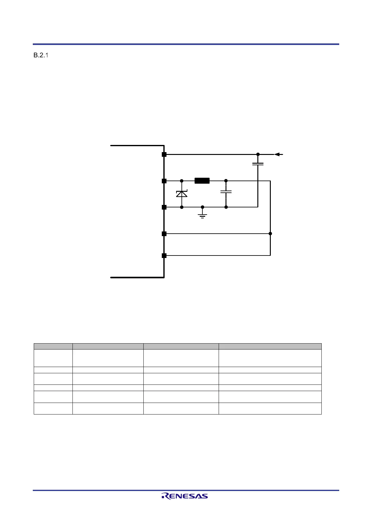
Wiring for the Switching Regulator
The following figure gives the recommendation of the wiring.
The switching regulator output (LX) delivers the 1.5 V voltage, that is smoothed with the external devices. This voltage is connected to pin V
DD1.5V.
The following external devices are necessary for the switching regulator:
Figure B-1 shows the wiring for the external regulator circuit if the regulator is used to generate the 1.5 V for the PHYs.
Notes:
• All components should be placed as close as possible to the TPS-1.
• Important: The characteristic of C1 is mandatory. A lower ESR will cause problems with the regulator oscillation.
TPS-
1
BVDD
Switching Regulator Input
(Pin J1, 3.3V)
VDD15
Supply 1.5V Input
(Pin K1)
Feedback Regulator
(Pin F1)
FB
LX
BGND (G1) /
AGND_REG (G2)
Regulator Ouput 1.5V
(Pin H1)
VDD 3.3V
L1 (10 uH)
C1
(22 uF;
Tantal)
D1
GND for Switching
Regulator
+
+
C2
(22 uF);
Ceramic or
Tantalum
(digital GND)
Figure B-1: Wiring of the switching regulator
Table B-1: Table B-1: Part Table for the Switching Regulator
ESR: 150–350 mΩ
TCJB226M010R0300 (AVX)
SBS005 (Sanyo)
STPS1L30UPBF (ST)
Evaluated with (Murata):
GRM32ER71A226KE20L
Evaluated with:
MCR18EZHFLR100 (ROHM)
To avoid the recommended tantalum capacitor it is possible to compose the needed characteristics with a series connection of a resistor and a ceramic
capacitor. If you use ceramic capacitors only C1 has to be replaced by a ceramic capacitor in connection with a series resistor. C2 did not need a series
resistor.