TPS-1 User’s Manual: Hardware Appendix. B Board Design Information
R19UH0081ED0107 Rev. 1.07 page 78 of 86
Jul 30, 2018
Board Design Recommendations for Ethernet PHY
Supply Voltage Circuitry
The on-chip PHYs of the TPS-1 require additional filtered operating voltages as shown in the table below.
Table B- 2: Supply Voltages Circuitry for Ethernet PHY
Pin Name Function Supply Voltage Generation
D14 P1VDDARXTX Analog port RX/TX power supply, 1.5 V (PHY port 1) Must be generated from VDD15
(1.5 V) via a filter.
Analog port RX/TX power supply, 1.5 V (PHY port 2)
G14 VDDAPLL Analog central power supply, 1.5 V
Analog central power supply, 3.3 V
Must be generated from VDD33
(3.3 V) via a filter.
E12 VDD33ESD Analog test power supply, 3.3 V
Core/IO via a filter or connected
to GND Core/IO at the far end
from TPS-1.
D12,
D13,
L12,
L13
AGND Analog GND for PHYs. Must be generated from digital
GND by filter.
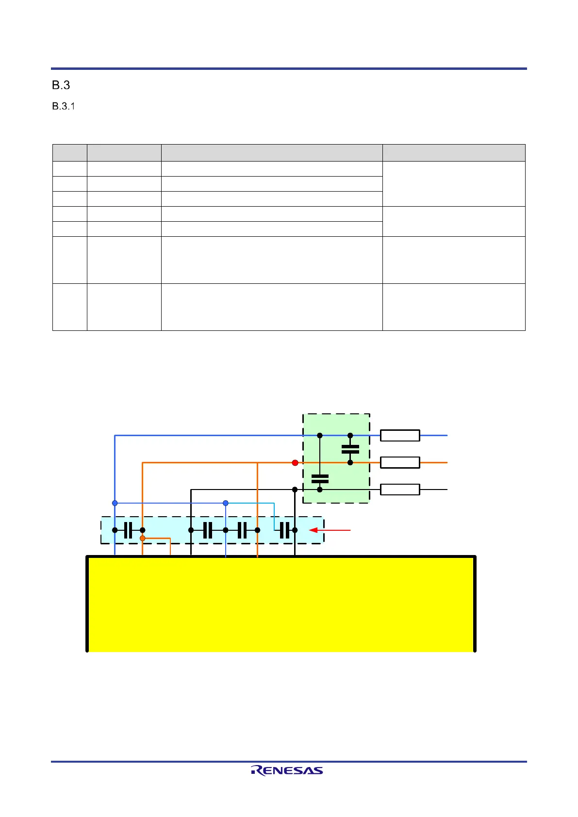
Besides filtering, the PHY-specific supply voltages should be equipped with pairs of decoupling capacitors. 10 nF and 22 nF capacitors should be used
for VDD33ESD, VDDAPLL, VDDACB and P(2:1)VDDARXTX. They should be placed as close as possible to the chip.
TPS-1
P1VDDARXTX
P2VDDARXTX
VDDAPLL
VDDACB
VDD33ESD
VSSAPLLCB
AGND
GND
VDD15
VDD33
Power Filters
Decoupling with
0.1 uF and 22 uF
Decoupling with 10 nF and 22 nF
(as close to the pins as possible)
Figure B-4: Decoupling capacitors for supply voltage
Additional pairs of 0.1 µF and 22 µF capacitors should be applied to VDD33ESD and P(2:1)VDDARXTX.
 Loading...