Theory of Operation-AA
501
The mainframe PNP transistor and 01522 form a
Darlington series-pass transistor. Frequency compensa-
tion for stability is provided by
R1520 and C1413. Current
limiting is accomplished by 01521 which senses the
current through
R1526. When the current delivered by the
-15 volt supply exceeds about 500
mA, 01521 turns on.
This shunts base drive current away from
(21522 and
lowers the output voltage of the power supply. Fuse
F1620
provides additional protection.
Im
option
@
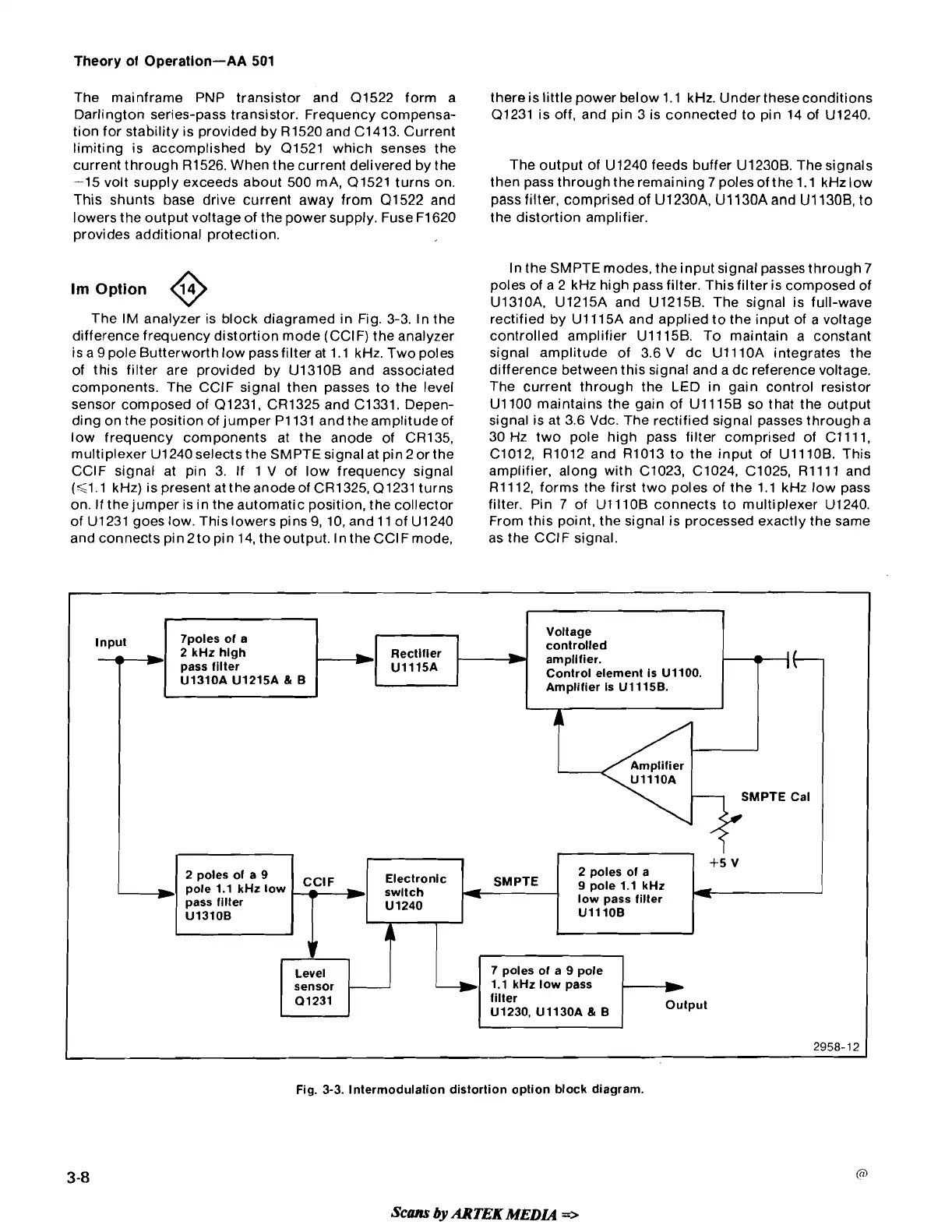
The IM analyzer is block diagramed in Fig. 3-3. In the
difference frequency distortion mode (CCIF) the analyzer
is a
9
pole Butterworth low pass filter at 1.1 kHz. Two poles
of this filter are provided by
U1310B and associated
components. The CCIF signal then passes to the level
sensor composed of 01231,
CR1325 and C1331. Depen-
ding on the position of jumper
PI 131 and theamplitudeof
low frequency components at the anode of
CR135,
multiplexer U1240 selects the SMPTE signal at pin 2 or the
CCIF signal at pin 3.
If
1 V of low frequency signal
(61.1 kHz) is present at theanodeof CR1325, Q1231 turns
on.
If
the jumper is in the automatic position, the collector
of
U1231 goes low. This lowers pins
9,
10, and 11 of U1240
and connects pin2to pin 14, theoutput. In theCCIFmode,
there is little power below 1.1 kHz. Under theseconditions
01231 is off, and pin 3 is connected to pin 14 of
U1240.
The output of U1240 feeds buffer U1230B. The signals
then pass through the remaining
7
poles of the 1.1 kHz low
pass filter, comprised of U1230A, U1130A and U1130B, to
the distortion amplifier.
In the SMPTE modes, the input signal passes through
7
poles of a 2 kHz high pass filter. This filter is composed of
U1310A, U1215A and U1215B. The signal is full-wave
rectified by
U1115A and applied to the input of a voltage
controlled amplifier
U1115B. To maintain a constant
signal amplitude of 3.6 V dc
U111OA integrates the
difference between this signal and a dc reference voltage.
The current through the LED in gain control resistor
U1100 maintains the gain of U1115B so that the output
signal is at 3.6 Vdc. The rectified signal passes through a
30 Hz two pole high pass filter comprised of
C1111.
C1012, R1012 and R1013 to the input of U111OB. This
amplifier, along with
C1023, C1024, C1025, R1111 and
R1112, forms the first two poles of the 1.1 kHz low pass
filter. Pin
7
of U111OB connects to multiplexer U1240.
From this point, the signal is processed exactly the same
as the CCIF signal.
Fig.
3-3.
Intermodulation distortion option block diagram.
Tpoles of a
Voltage
Input
2
kHz
high
controlled
Rectifier
I
I
pass fllter
U1115A
D
amplifier.
-
U1310A U1215A
&
B
Control element is
U1100.
Amplifier is
U1115B.
SMPTE Cal
pole
1.1
HZ
tow
*
pass filter
U1310B
2
poles of a
9
pole
1.1
HZ
low pass filter
UlllOB
Electronic
sw~tch SMPTE
U 1240
+5
v
*
A
.
Level
sensor
01231
filter
U1230, U1130A
&
B
Output
2958-
12
 Loading...