10 www.xilinx.com VC707 Evaluation Board
UG885 (v1.4) May 12, 2014
Chapter 1: VC707 Evaluation Board Features
Feature Descriptions
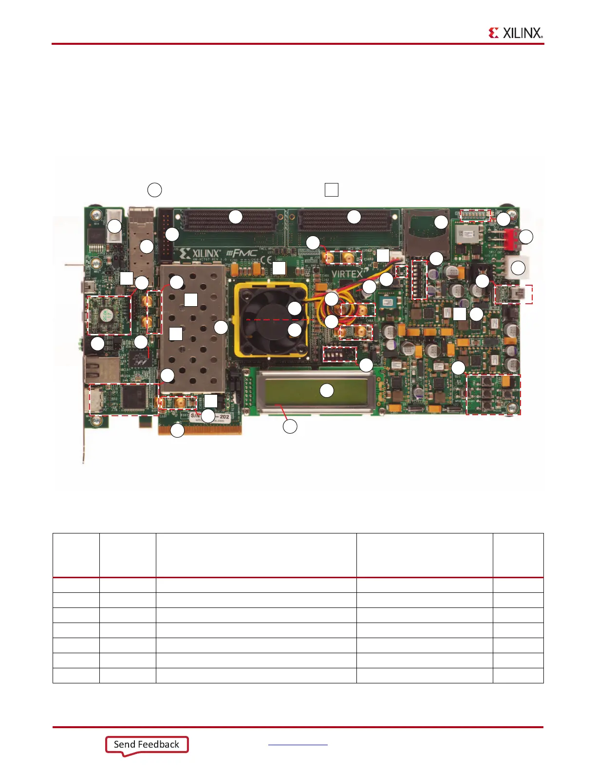
Figure 1-2 shows the VC707 board. Each numbered feature that is referenced in Figure 1-2
is described in the sections that follow.
Note:
The image in Figure 1-2 is for reference only and might not reflect the current revision of the
board.
X-Ref Target - Figure 1-2
Figure 1-2: VC707 Board Component Locations
30
31
33
21
32
26
35
34
32
27
19
22
24
23
User rotary switch
located under LCD
25
20
28
29
18
13
15
16
2
7
6
17
14
1
8
12
10
3
9
11
5
4
00
Square callout references a component
on the back side of the board
Round callout references a component
on the front side of the board
00
UG885_c1_02_070913
36
37
Table 1-1: VC707 Board Component Descriptions
Callout
Reference
Designator
Component Description Notes
Schematic
0381418
Page
Number
1 U1 Virtex-7 FPGA with cooling fan XC7VX485T-2FFG1761C
2 J1 DDR3 SODIMM memory (1 GB) Micron MT8JTF12864HZ-1G6G1 21
3 U3 BPI parallel NOR flash memory (1 Gb) Micron PC28F00AG18FE 35
4 U8, J2 USB ULPI transceiver, USB mini-B connector SMSC USB3320-EZK 44
5 U29 SD card interface connector Molex 67840-8001 37
6 U26 USB JTAG interface, USB micro-B connector Digilent USB JTAG module 20
7 U51 System clock, 200 MHz, LVDS (back side of board) SiTime SIT9102-243N25E200.0000 32

 Loading...


