48 www.xilinx.com VC707 Evaluation Board
UG885 (v1.4) May 12, 2014
Chapter 1: VC707 Evaluation Board Features
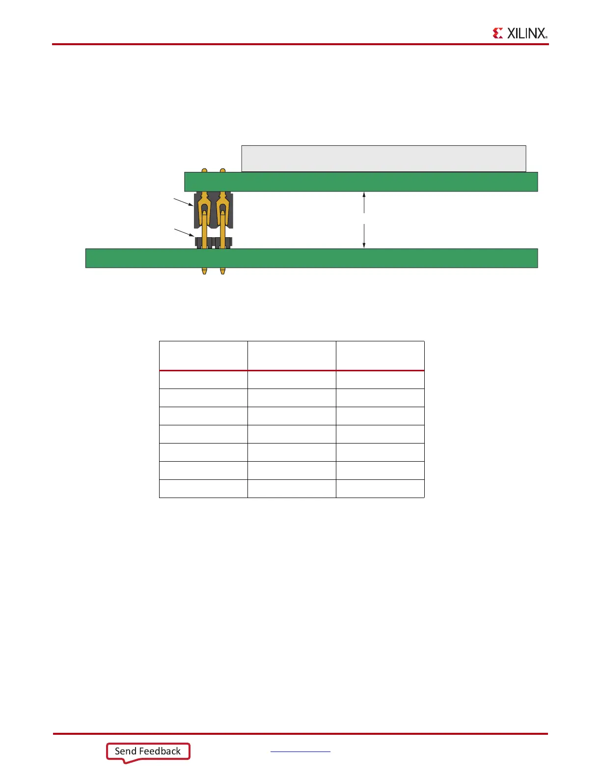
The VC707 board base board uses a male Samtec MTLW-107-07-G-D-265 2x7 header (J23)
with 0.025-inch square posts on 0.100-inch centers for connecting to a Samtec
SLW-107-01-L-D female socket on the LCD display panel assembly. The LCD header
shown in Figure 1-21. When the LCD is not installed, the J31 header pins listed in
Table 1-23 are available for use as GPIO.
Table 1-23 lists the connections between the FPGA and the LCD header.
References
The data sheet for the Displaytech S162DBABC LCD can be found at the Displaytech
website [Ref 23]. Choose the S162D model full spec download arrow.
I
2
C Bus
[Figure 1-2, callout 20]
The VC707 board implements a single I
2
C port on the FPGA (IIC_SDA_MAIN,
IIC_SDA_SCL), which is routed through a 1-to-8 channel I
2
C bus switch (U52). The bus
switch can operate at speeds up to 400 kHz.
The bus switch I
2
C address is 0x74 (0b01110100) and must be addressed and configured
to select the desired downstream device.
X-Ref Target - Figure 1-21
Figure 1-21: LCD Header Details
UG885_c1_21_021412
LCD Display Assembly
VC707 PWA
10 mm
Low Profile Socket
Samtec SLW-107-01-L-D
Low Profile Terminal
Samtec MTLW-107-07-G-D-265
Table 1-23: FPGA to LCD Header Connections
FPGA (U1)
Pin
Net Name
LCD Header Pin
(J31)
AT42 LCD_DB4_LS 4
AR38 LCD_DB5_LS 3
AR39 LCD_DB6_LS 2
AN40 LCD_DB7_LS 1
AR42 LCD_RW_LS 10
AN41 LCD_RS_LS 11
AT40 LCD_E_LS 9

 Loading...


