VC707 Evaluation Board www.xilinx.com 49
UG885 (v1.4) May 12, 2014
Feature Descriptions
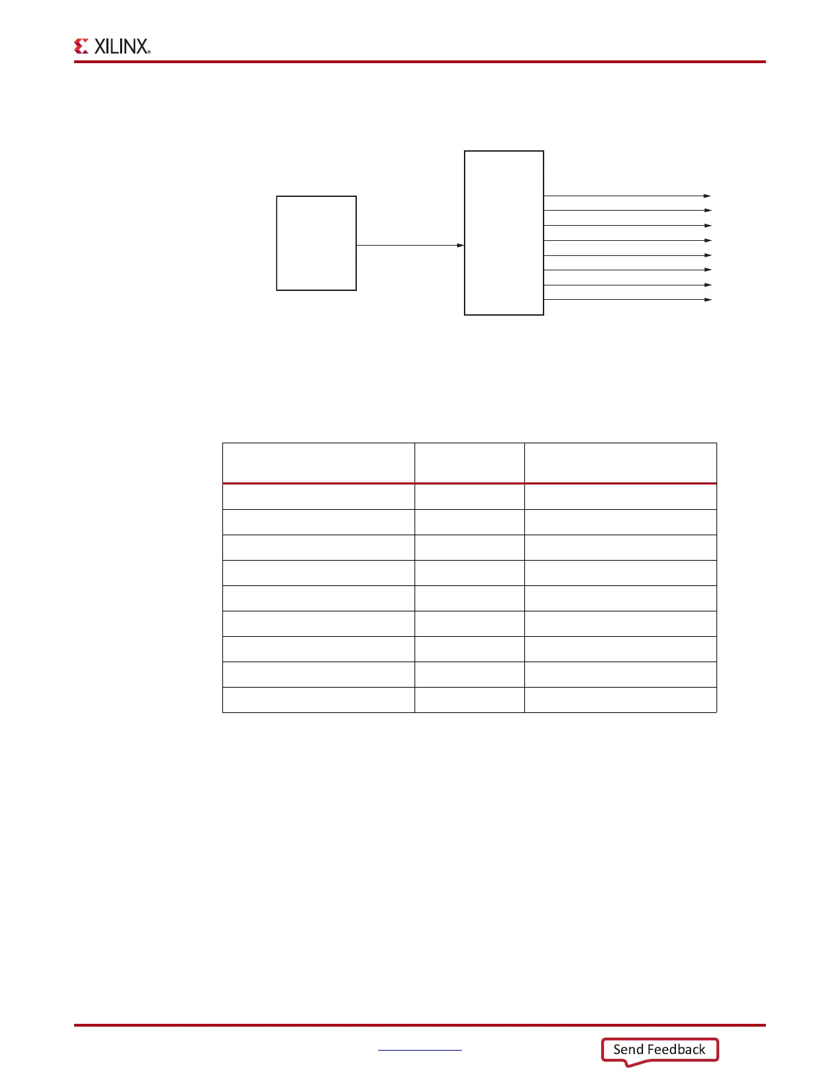
The VC707 board I
2
C bus topology is shown in Figure 1-22.
User applications that communicate with devices on one of the downstream I
2
C buses
must first set up a path to the desired bus through the U52 bus switch at I
2
C address 0x74
(0b01110100). Table 1-24 lists the address for each bus.
Information about the PCA9548 is available on the TI Semiconductor website [Ref 24].
X-Ref Target - Figure 1-22
Figure 1-22: I
2
C Bus Topology
Table 1-24: I
2
C Bus Addresses
I
2
C Bus
I
2
C Switch
Position
I
2
C Address
PCA9548 NA 0b1110100
USER_CLK_SDL/SCL 0 0b1110000
FMC1_HPC_IIC_SDA/SCL 1 0bXXXXX00
FMC2_HPC_IIC_SDA/SCL 2 0bXXXXX00
EEPROM_IIC_SDA/SCL 3 0b1010100
SFP_IIC_SDA/SCL 4 0b1010000
IIC_SDA/SCL_HDMI 5 0b0111001
IIC_SDA/SCL_DDR3 6 0b1010000, 0b0011000
Si5324_SDA/SCL 7 0b1010000
Notes:
1. Use the PCA9458 (U52) at I
2
C address 0x74 (0b01110100) to setup the path to these buses.
PCA9548
1
2
C 1-to-8
Bus Switch
CH7 - SI5324_SDA/SCL
U52
IIC_SDA/SCL_MAIN
CH6 - IIC_SDA/SCL_DDR3
CH5 - IIC_SDA/SCL_HDMI
CH4 - SFP_IIC_SDA/SCL
CH3 - EEPROM_IIC_SDA/SCL
CH2 - FMC2_HPC_IIC_SDA/SCL
CH1 - FMC1_HPC_IIC_SDA/SCL
CH0 - USER_CLK_SDL/SCL
FPGA
Bank 15
(2.5V)
U1
UG855_C1_22_021012

 Loading...


