12 www.xilinx.com VC707 Evaluation Board
UG885 (v1.4) May 12, 2014
Chapter 1: VC707 Evaluation Board Features
Virtex-7 XC7VX485T-2FFG1761C FPGA
[Figure 1-2, callout 1]
The VC707 board is populated with the Virtex-7 XC7VX485T-2FFG1761C FPGA.
For further information on Virtex-7 FPGAs, see
7 Series FPGAs Overview (DS180) [Ref 1].
To determine the type of FPGA resident on the VC707 board, refer to the Master Answer
Record listed in Appendix F: References.
FPGA Configuration
The VC707 board supports two of the five 7 series FPGA configuration modes:
• Master BPI using the onboard Linear BPI Flash memory
• JTAG using a type-A to micro-B USB cable for connecting the host PC to the VC707
board configuration port
Each configuration interface corresponds to one or more configuration modes and bus
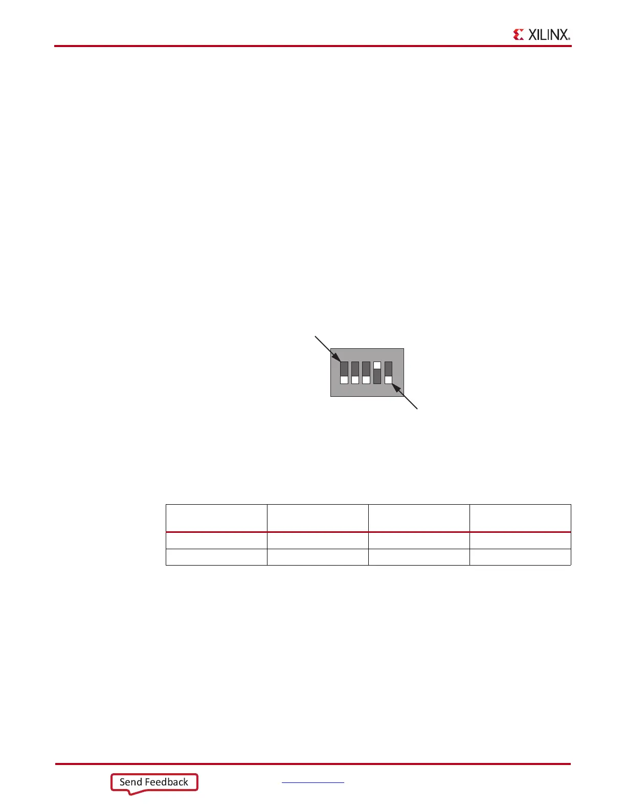
widths as listed in Table 1-2. The mode switches M2, M1, and M0 are on SW11 positions 3,
4, and 5 respectively as shown in Figure 1-3.
The default mode setting is M[2:0] = 010, which selects Master BPI at board power-on. See
Configuration Options, page 77 for detailed information about the mode switch SW11.
For full details on configuring the FPGA, see 7 Series FPGAs Configuration User Guide
(UG470) [Ref 2].
X-Ref Target - Figure 1-3
Figure 1-3: SW11 Default Settings
Table 1-2: VC707 Board FPGA Configuration Modes
Configuration
Mode
SW13 DIP switch
Settings (M[2:0])
Bus
Width
CCLK
Direction
Master BPI 010 x8, x16 Output
JTAG 101 x1 Not Applicable
UG885_c1_03_020612
1
OFF Position = 0
ON Position = 1
2345
A25
A24
M2
M1
M0

 Loading...


