VC707 Evaluation Board www.xilinx.com 13
UG885 (v1.4) May 12, 2014
Feature Descriptions
I/O Voltage Rails
There are 17 I/O banks available on the Virtex-7 device. Sixteen I/O banks are available on
the VC707 board, bank 31 is not used. The voltages applied to the FPGA I/O banks used by
the VC707 board are listed in Table 1-3.
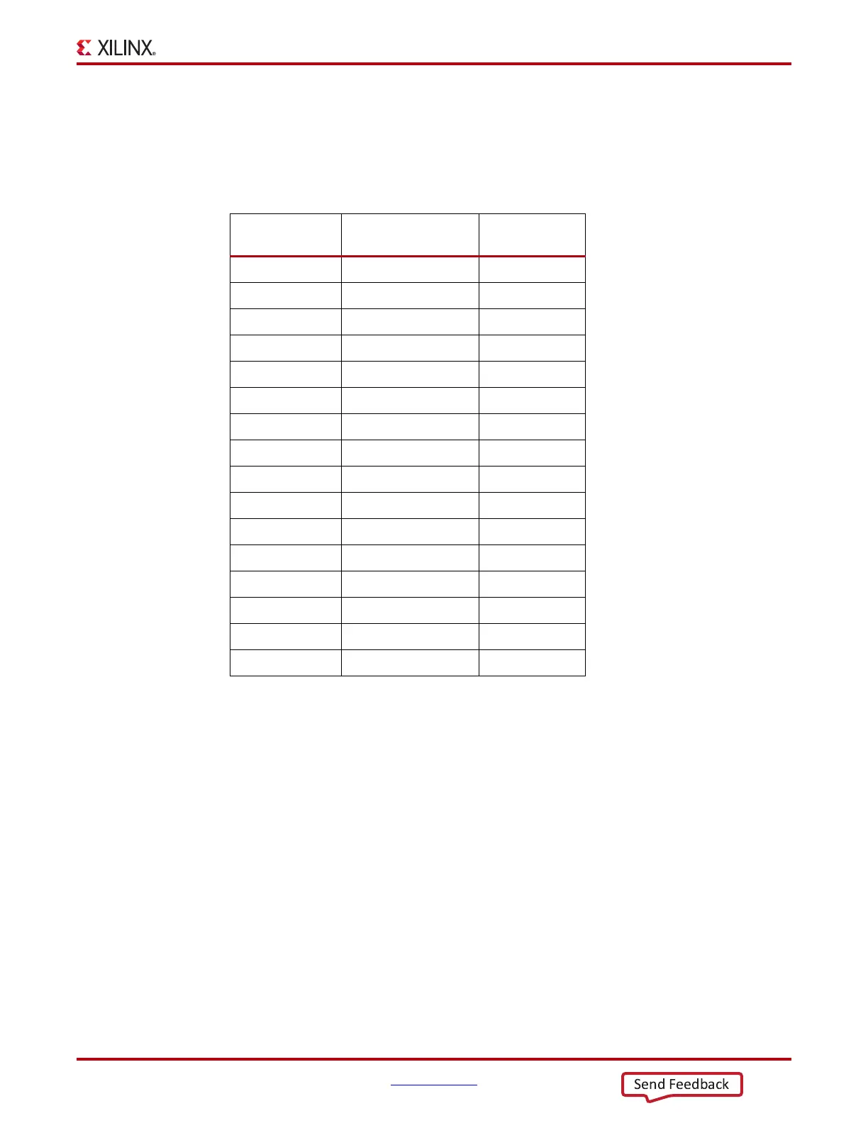
Table 1-3: I/O Voltage Rails
FPGA (U1)
Bank
Power Supply Rail
Net Name
Voltage
Bank 0 VCC1V8_FPGA 1.8V
Bank 13 VCC1V8_FPGA 1.8V
Bank 14 VCC1V8_FPGA 1.8V
Bank 15 VCC1V8_FPGA 1.8V
Bank 16
(1)
VADJ_FPGA 1.8V (default)
Bank 17
(1)
VADJ_FPGA 1.8V (default)
Bank 18
(1)
VADJ_FPGA 1.8V (default)
Bank 19
(1)
VADJ_FPGA 1.8V (default)
Bank 31 NOT USED NA
Bank 33 VCC1V8_FPGA 1.8V
Bank 34 VADJ_FPGA 1.8V (default)
Bank 35 VADJ_FPGA 1.8V (default)
Bank 36 FMC1_VIO_B_M2C Variable
Bank 37 VCC1V5_FPGA 1.5V
Bank 38 VCC1V5_FPGA 1.5V
Bank 39 VCC1V5_FPGA 1.5V
Notes:
1. The VADJ_FPGA rail can support up to 1.8V due to FPGA HP
bank connections to FMC. For more information on
VADJ_FPGA see Power Management, page 69.

 Loading...


