80 www.xilinx.com VC707 Evaluation Board
UG885 (v1.4) May 12, 2014
Appendix A: Default Switch and Jumper Settings
Configuration DIP Switch SW11
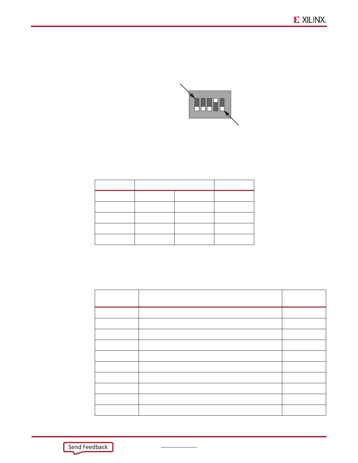
See Figure 1-2, page 10 Item 29 for location of SW11. Default settings are shown in
Figure A-2 and details are listed in Table A-2.
The default mode setting M[2:0] = 010 selects Master BPI configuration at board
power-on.
Default Jumper Settings
See Figure 1-2, page 10 for locations of jumpers listed in Table A-3.
X-Ref Target - Figure A-2
Figure A-2: SW11 Default Settings
Tab le A- 2: SW11 Default Switch Settings
Position Function Default
1 FLASH_A25 A25 Off
2 FLASH_A24 A24 Off
3FPGA_M2 M0 Off
4FPGA_M1 M1 On
5FPGA_M0 M3 Off
UG885_aB_02_020612
1
OFF Position = 0
ON Position = 1
2345
A25
A24
M2
M1
M0
Tab le A- 3: Default Jumper Settings
Jumper Function
Default Jumper
Position
J6 SFP Enable None
J9 XADC GND ferrite filter bypass jumper None
J10 XADC GND-to-XADC_AGND jumper 1–2
J11 TI Controller U42 Addr 52 Reset jumper None
J12 TI Controller U43 Addr 53 Reset jumper None
J13 USB Mini-B Connector J2 VBUS None
J14 USB SMBC U8 CLKOUT selector None
J38 SFP RX Rate: 1-2 = Full BW Rate, 2-3 = Low BW Rate 1–2
J39 SFP TX Rate: 1-2 = Full BW Rate, 2-3 = Low BW Rate 1–2
J42 XADC external 1.2V or internal VREFP selector 1–2

 Loading...


