18 www.xilinx.com VC707 Evaluation Board
UG885 (v1.4) May 12, 2014
Chapter 1: VC707 Evaluation Board Features
The VC707 DDR3 SODIMM interface adheres to the constraints guidelines in the DDR3
Design Guidelines section of 7 Series FPGAs Memory Interface Solutions User Guide (UG586)
[Ref 3]. The VC707 DDR3 SODIMM interface is a 40Ω impedance implementation. Other
memory interface details are available in UG586 and 7 Series FPGAs Memory Resources
User Guide (UG473) [Ref 4].
Linear BPI Flash Memory
[Figure 1-2, callout 3]
The Linear BPI Flash memory located at U3 provides 128 MB of nonvolatile storage that
can be used for configuration or software storage. The data, address, and control signals
are connected to the FPGA. The BPI Flash memory device is packaged in a 64-pin BGA.
• Part number: PC28F00AG18FE (Micron)
• Supply voltage: 1.8V
• Datapath width: 16 bits (26 address lines and 7 control signals)
• Data rate: Up to 80 MHz
The Linear BPI Flash memory can synchronously configure the FPGA in Master BPI mode
at the 80 MHz data rate supported by the PC28F00AG18FE flash memory. The fastest
configuration method uses the external 80 MHz oscillator connected to the FPGA's
EMCCLK pin.
Multiple bitstreams can be stored in the Linear BPI Flash. The two most significant address
bits (A25, A24) of the flash memory are connected to DIP switch SW11 positions 1 and 2
respectively, and to the RS1 and RS0 pins of the FPGA. By placing valid XC7VX485T
bitstreams at four different offset addresses in the flash memory, 1 of the 4 bitstreams can
be selected to configure the FPGA by appropriately setting the DIP switch SW11. The
connections between the BPI Flash memory and the FPGA are listed in Table 1-5.
K19 DDR3_CKE0 73 CKE0
J18 DDR3_CKE1 74 CKE1
G18 DDR3_CLK0_N 103 CK0_N
H19 DDR3_CLK0_P 101 CK0_P
F19 DDR3_CLK1_N 104 CK1_N
G19 DDR3_CLK1_P 102 CK1_P
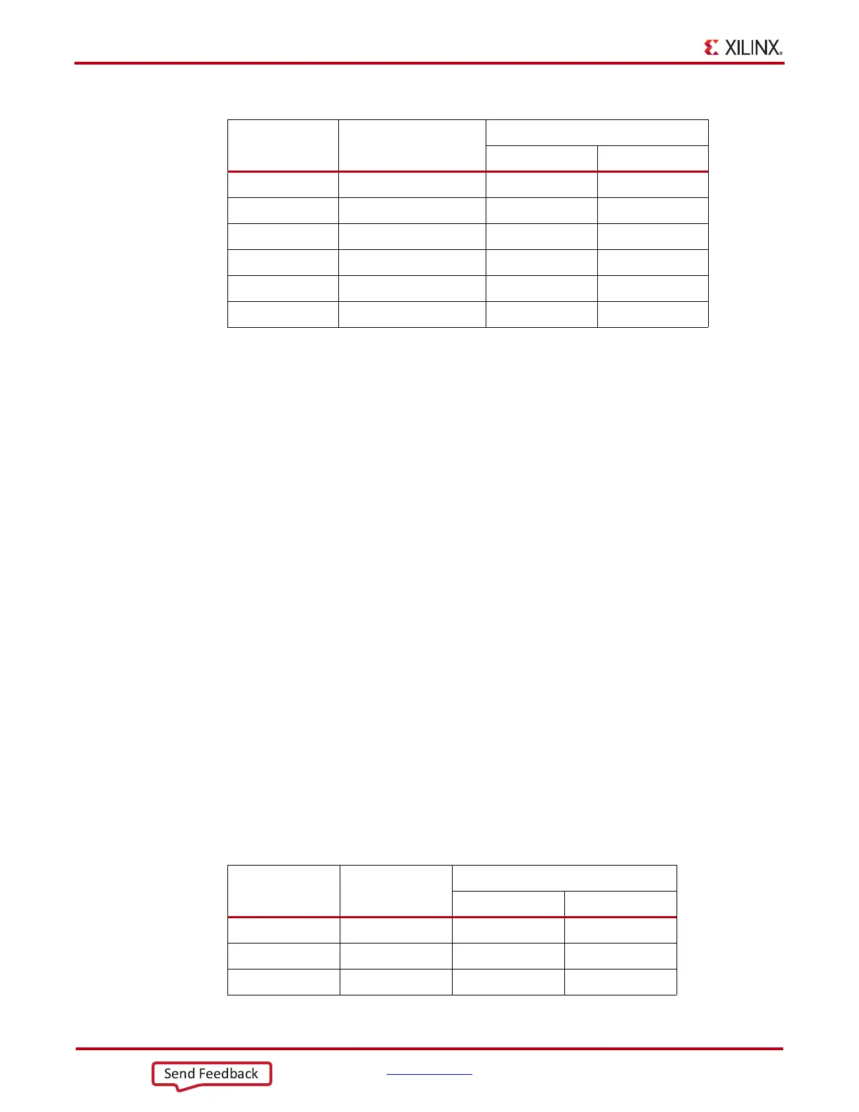
Table 1-4: DDR3 Memory Connections to the FPGA (Cont’d)
FPGA (U1)
Pin
Net Name
J1 DDR3 Memory
Pin Number Pin Name
Table 1-5: BPI Flash Memory Connections to the FPGA
FPGA (U1) Pin Net Name
BPI Flash Memory (U3)
Pin Number Pin Name
AJ28 FLASH_A0 A1 A1
AH28 FLASH_A1 B1 A2
AG31 FLASH_A2 C1 A3

 Loading...


