VC707 Evaluation Board www.xilinx.com 69
UG885 (v1.4) May 12, 2014
Feature Descriptions
Power Management
The VC707 board power distribution diagram is shown in Figure 1-33.
The PCB layout and power system meet the recommended criteria described in
7 Series FPGAs PCB Design and Pin Planning Guide (UG483) [Ref 9].
K38 FMC2_HPC_HB17_CC_N AW17
J39 FMC2_VIO_B_M2C BANK
32
VCCO
K40 FMC2_VIO_B_M2C BANK 32
VCCO
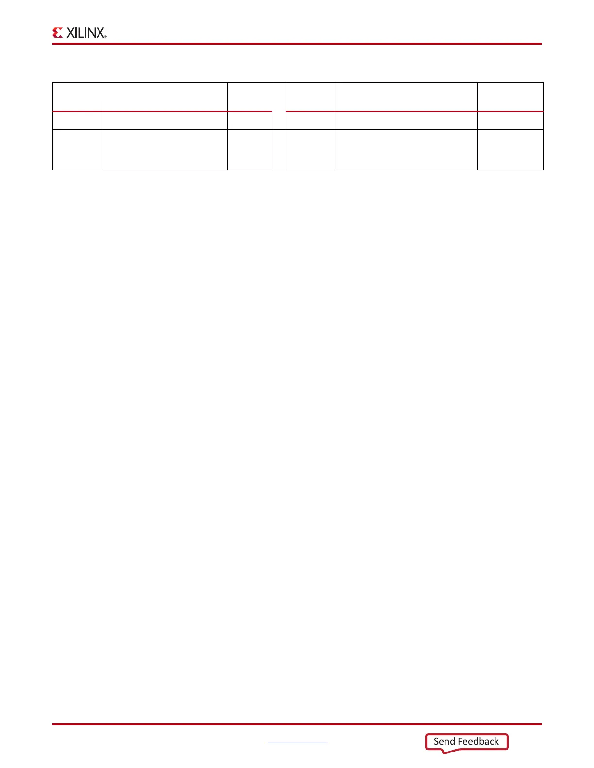
Table 1-28: J37 VITA 57.1 FMC 2 HPC Connections (Cont’d)
J37 FMC 2
HPC Pin
Schematic Net Name
U1 FPGA
Pin
J37 FMC 2
HPC Pin
Schematic Net Name U1 FPGA Pin

 Loading...


