32 www.xilinx.com VC707 Evaluation Board
UG885 (v1.4) May 12, 2014
Chapter 1: VC707 Evaluation Board Features
See the Silicon Labs Si5324 data sheet for more information on this device [Ref 19].
GTX Transceivers
[Figure 1-2, callout 12]
The VC707 board provides access to 27 GTX transceivers:
• Eight of the GTX transceivers are wired to the PCI Express x8 endpoint edge
connector (P1) fingers
• Eight of the GTX transceivers are wired to the FM1 HPC connector (J35)
• Eight of the GTX transceivers are wired to the FMC2 HPC connector (J37)
• One GTX is wired to SMA connectors (RX: J27, J28 TX: J29, J30)
• One GTX is wired to the SFP/SFP+ Module connector (P3)
• One GTX is used for the SGMII connection to the Ethernet PHY (U50)
The GTX transceivers in 7 series FPGAs are grouped into four channels described as
Quads. The reference clock for a Quad can be sourced from the Quad above or Quad below
the GTX Quad of interest. There are four GTX Quads on the VC707 board with connectivity
as shown here:
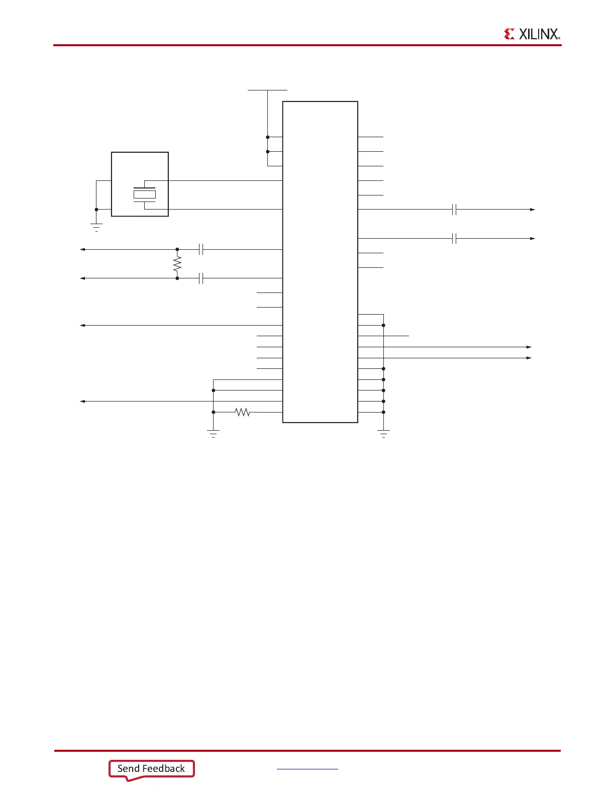
X-Ref Target - Figure 1-13
Figure 1-13: Jitter Attenuated Clock
UG885_c1_13_021412
R16
4.7KΩ 5%
SI5324_VCC
Si5324C-C-GM
Clock Multiplier/
Jitter Attenuator
VDD3
GND
XB
XA
NC5
32
6
30
29
28
U24
CKOUT1_N
7
33
CKOUT1_P
C31
0.1μF 25V
X5R
C32
0.1μF 25V
X5R
SI5326_XTAL_XA
GND2
GND1
XB
XA
X6
114.285 MHz
20 ppm
SI5326_OUT_C_N
SI5326_OUT_C_P
SI5326_OUT_N
SI5326_OUT_P
SI5326_XTAL_XB
GND
NC4
2
1
3
4
C33
0.1μF 25V
X5R
C34
0.1μF 25V
X5R
REC_CLOCK_P
REC_CLOCK_N
REC_CLOCK_C_P
REC_CLOCK_C_N
16
17
R167
100Ω
CKIN1_P
CKIN1_N
NC
NC
12
13
CKIN2_P
CKIN2_N
10
5
VDD2
VDD1
14
NC3
9
NC2
2
NC1
NC
NC
NC
NC
NC
35
34
NC
NC
CKOUT2_P
CKOUT2_N
SI5326_INT_ALM 3
NC 4
NC 11
NC 15
NC 18
19
20
SI5326_RST 1
21
31
GND2
9
GND1
31
A2_SS
31
A1
24
A0
22
SI5326_SCL
SCL
23
SI5326_SDA
SDA_SDO
27
NC
SDI
36
CMODE
GND
GND4
GND3
LOL
RATE1
RATE0
C2B
INT_C1B
CS_CA
RST_B
37
GNDPAD

 Loading...


