22 www.xilinx.com VC707 Evaluation Board
UG885 (v1.4) May 12, 2014
Chapter 1: VC707 Evaluation Board Features
USB 2.0 ULPI Transceiver
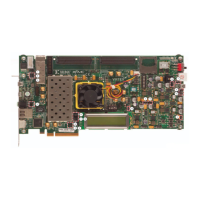
[Figure 1-2, callout 4]
The VC707 board uses a Standard Microsystems Corporation USB3320 USB 2.0 ULPI
Transceiver (U8) to support a USB connection to the host computer. A USB cable is
supplied in the VC707 Evaluation Kit (type-A connector to host computer, mini-B
connector to VC707 board connector J2).
The USB3320 is a high-speed USB 2.0 PHY supporting the UTMI+ low pin interface (ULPI)
interface standard. The ULPI standard defines the interface between the USB controller IP
and the PHY device which drives the physical USB bus. Use of the ULPI standard reduces
the interface pin count between the USB controller IP and the PHY device.
The USB3320 is clocked by a 24 MHz crystal. The ULPI interface supports two clocking
modes selected by jumper on J14:
• 24 MHz ULPI output clock mode (default): No jumper on J14. The PHY drives the
UPLI clock. This is the default setting.
• 60 MHz ULPI input clock mode: Jumper across J14 pins 1–2.
Consult the SMSC USB3320 data sheet for clocking mode details [Ref 17].
The FPGA interface to the USB3320 transceiver is implemented through the AXI universal
serial bus 2.0 device IP. See LogiCORE IP AXI Universal Serial Bus 2.0 Device Product Guide
for Vivado Design Suite (PG137) [Ref 5]
Note:
The AXI universal serial bus 2.0 device IP supports USB-supplied power mode only. Jumpers
on headers J13 and J45 must be configured to their default state as described here:
•J13=jumper removed
• J45 = jumper across pins 1–2
Figure 1-5 shows the shield for the USB mini-B connector (J2) can be tied to GND by a
jumper on header J44 pins 1–2 (default). The USB shield can optionally be connected
through a capacitor to GND by installing a tantalum capacitor (body size C) at location
C326 and jumping pins 2-3 on header J44.
 Loading...
