VC707 Evaluation Board www.xilinx.com 55
UG885 (v1.4) May 12, 2014
Feature Descriptions
Switches
[Figure 1-2, callout 27 - 28]
The VC707 board Evaluation Board includes a power and a configuration switch:
• Power On/Off Slide Switch SW12 (callout 27)
• FPGA_PROG_B SW9, active-Low (callout 28)
Power On/Off Slide Switch SW12
[Figure 1-2, callout 27]
The VC707 board power switch is SW12. Sliding the switch actuator from the Off to On
position applies 12V power from J18, a 6-pin mini-fit connector. Green LED DS16
illuminates when the VC707 board power is on. See Power Management for details on the
onboard power system.
Caution!
Do NOT plug a PC ATX power supply 6-pin connector into J18 on the VC707 board.
The ATX 6-pin connector has a different pinout than J18. Connecting an ATX 6-pin connector into
J18 will damage the VC707 board and void the board warranty.
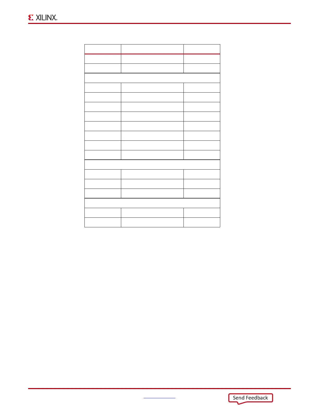
AW40 GPIO_SW_W SW7.3
AV39 GPIO_SW_C SW6.3
8-Pole DIP Switch
AV30 GPIO_DIP_SW0 SW2.16
AY33 GPIO_DIP_SW1 SW2.15
BA31 GPIO_DIP_SW2 SW2.14
BA32 GPIO_DIP_SW3 SW2.13
AW30 GPIO_DIP_SW4 SW2.12
AY30 GPIO_DIP_SW5 SW2.11
BA30 GPIO_DIP_SW6 SW2.10
BB31 GPIO_DIP_SW7 SW2.9
User Rotary Switch
AT31 ROTARY_INCB SW10.6
AW31 ROTARY_PUSH SW10.5
AR33 ROTARY_INCA SW10.1
User SMA
AN31 USER_SMA_GPIO_P J33.1
AP31 USER_SMA_GPIO_N J34.1
Table 1-26: GPIO Connections to FPGA U1 (Cont’d)
FPGA (U1) Pin Schematic Net Name GPIO Pin

 Loading...


