54 www.xilinx.com VC707 Evaluation Board
UG885 (v1.4) May 12, 2014
Chapter 1: VC707 Evaluation Board Features
User SMA
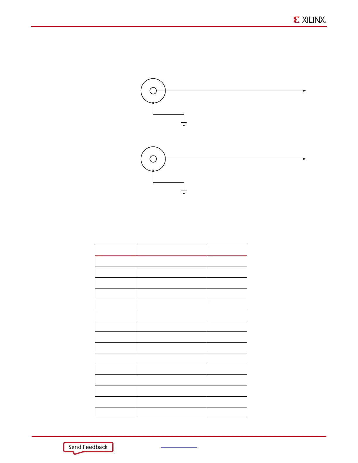
Figure 1-28 shows the user SMA circuit.
Table 1-26 lists the GPIO Connections to FPGA U1.
X-Ref Target - Figure 1-28
Figure 1-28: User SMA
Table 1-26: GPIO Connections to FPGA U1
FPGA (U1) Pin Schematic Net Name GPIO Pin
Indicator LEDs (Active-High)
AM39 GPIO_LED_0 DS2.2
AN39 GPIO_LED_1 DS3.2
AR37 GPIO_LED_2 DS4.2
AT37 GPIO_LED_3 DS5.2
AR35 GPIO_LED_4 DS6.2
AP41 GPIO_LED_5 DS7.2
AP42 GPIO_LED_6 DS8.2
AU39 GPIO_LED_7 DS9.2
CPU Reset Pushbutton Switch
AV40 CPU_RESET SW3.3
Directional Pushbutton Switches
AR40 GPIO_SW_N SW3.3
AU38 GPIO_SW_E SW4.3
AP40 GPIO_SW_S SW5.3
GND
UG885_c1_126_012413
USER SMA GPIO P
J33
SMA
Connector
GND
USER SMA GPIO N
J34
SMA
Connector

 Loading...


