Do you have a question about the Xilinx Virtex UltraScale+ FPGAs and is the answer not in the manual?
| Brand | Xilinx |
|---|---|
| Model | Virtex UltraScale+ FPGAs |
| Category | Transceiver |
| Language | English |
Key features of the GTM transceiver, including supported line rates and modulation.
Description of the wizard tool for configuring GTM transceivers.
Explanation of reference clock input options and selection architecture.
Steps for initializing the GTM transceiver TX and RX datapaths.
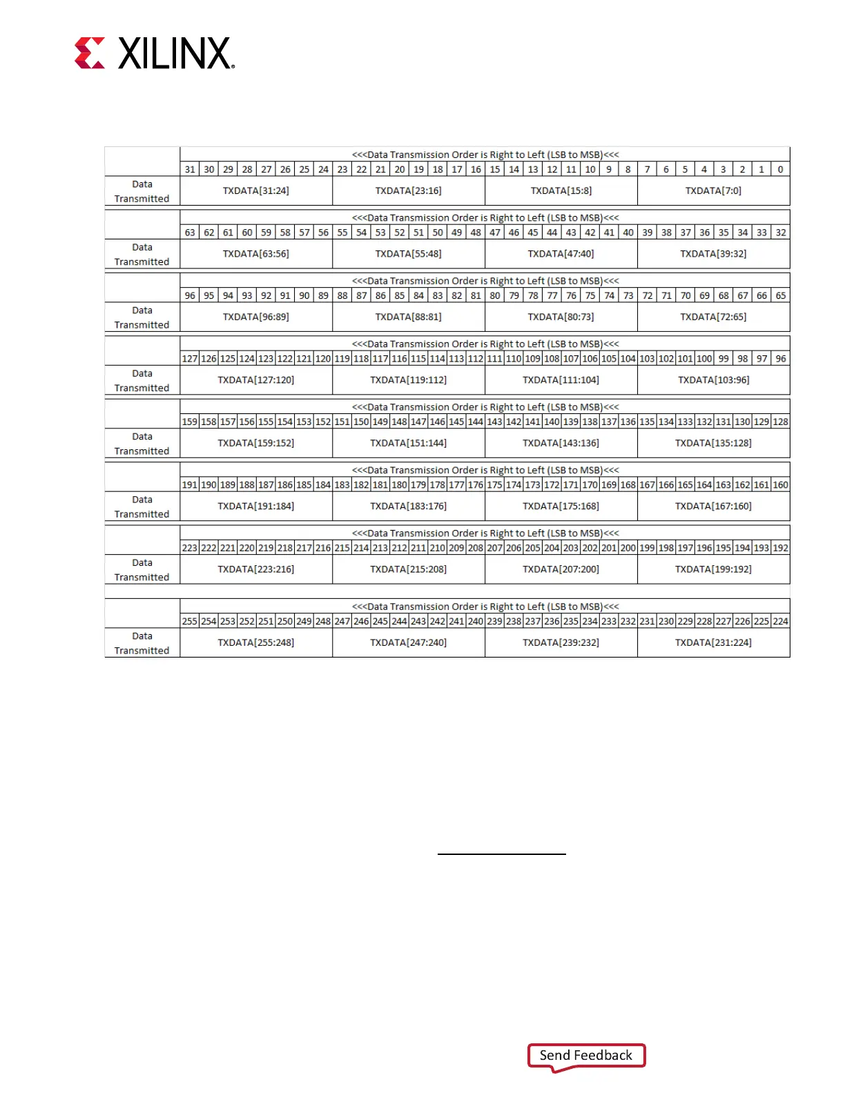
Gateway to the TX datapath, including data width and clocking.
Details on the Integrated KP4 Reed-Solomon Forward Error Correction.
Generates industry-standard PRBS patterns for signal integrity testing.
Controls output buffer characteristics like voltage and pre-emphasis.
Compensates for channel attenuation and distortion using CTLE, FFE, and DFE.
Clock Data Recovery circuit for extracting clock and data from incoming streams.
Details on the Integrated KP4 Reed-Solomon Forward Error Correction.
Gateway to the RX datapath, including data width and clocking.

