ZCU111 Board User Guide 97
UG1271 (v1.1) August 6, 2018 www.xilinx.com
Appendix D: HW-FMC-XM500
ADC/DAC Bank Data and Clock Channel Mapping
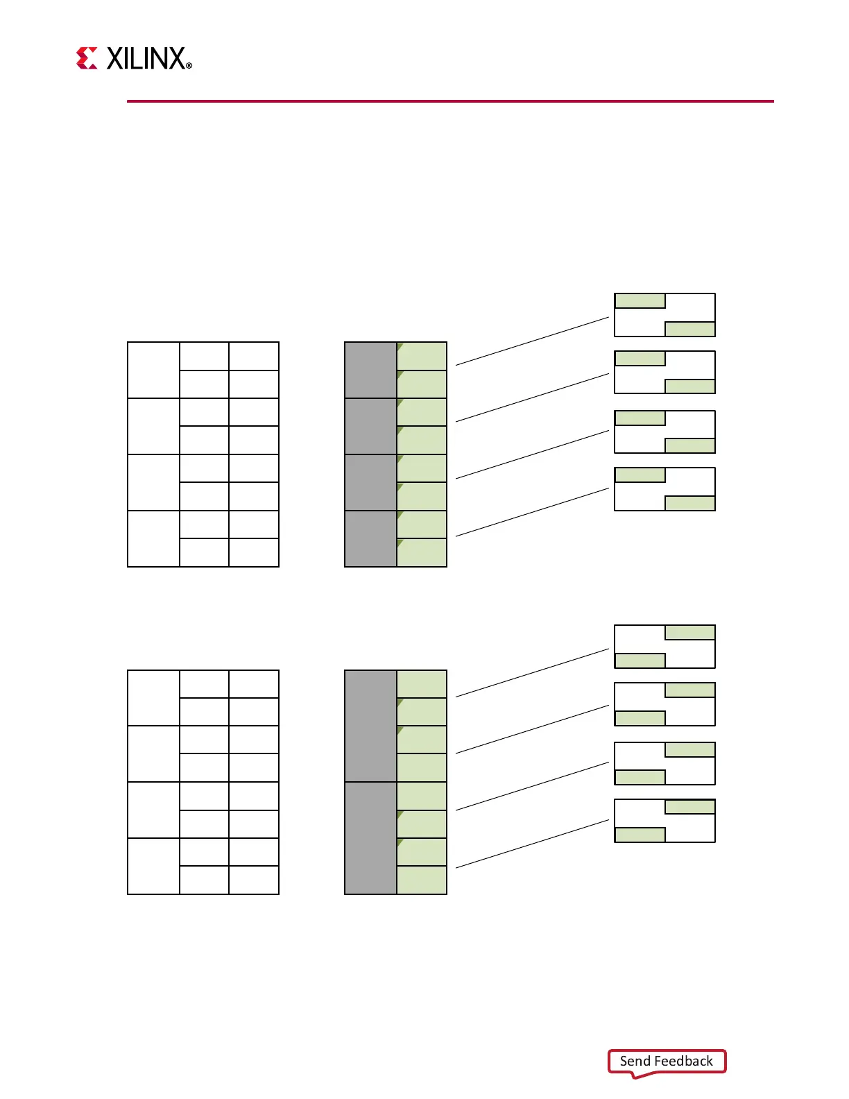
This section provides details on the ZCU111 board U1 RFSoC ZCU28DR ADC/DAC bank data
and clock channel mapping. Figure D-3 and Figure D-4 show the ZCU111 board U1 RFSoC
ZC28DR bank RF channel mapping and RF bank connectivity.
X-Ref Target - Figure D-3
Figure D-3: RFSoC ZCU28DR ADC/DAC Bank Channel Mapping
FPGA
ADC_00
ADC_01
ADC_02
ADC_03
ADC_04
ADC_05
ADC_06
ADC_07
AMC
DAC_00
DAC_01
DAC_02
DAC_03
DAC_04
DAC_05
DAC_06
DAC_07
224
0
2
1
3
225
0
2
1
3
226
0
2
1
3
227
0
2
1
3
224
01
23
225
01
23
226
01
23
227
01
23
228
0
2
1
3
229
0
2
1
3
230
0
2
1
3
231
0
2
1
3
228
0
1
2
3
0
1
229
2
3
X21082-062118

 Loading...


