ZCU111 Board User Guide 99
UG1271 (v1.1) August 6, 2018 www.xilinx.com
Appendix D: HW-FMC-XM500
XM500 ADC/DAC Data and Clock SMA
This section provides details on the XM500 ADC/DAC data and clock SMA, and I/O 2x10
header connectors to the ZCU111 board U1 RFSoC ZCU28DR channel mapping. Tabl e D-2
provides the XM500 ADC/DAC data and clock mapping.
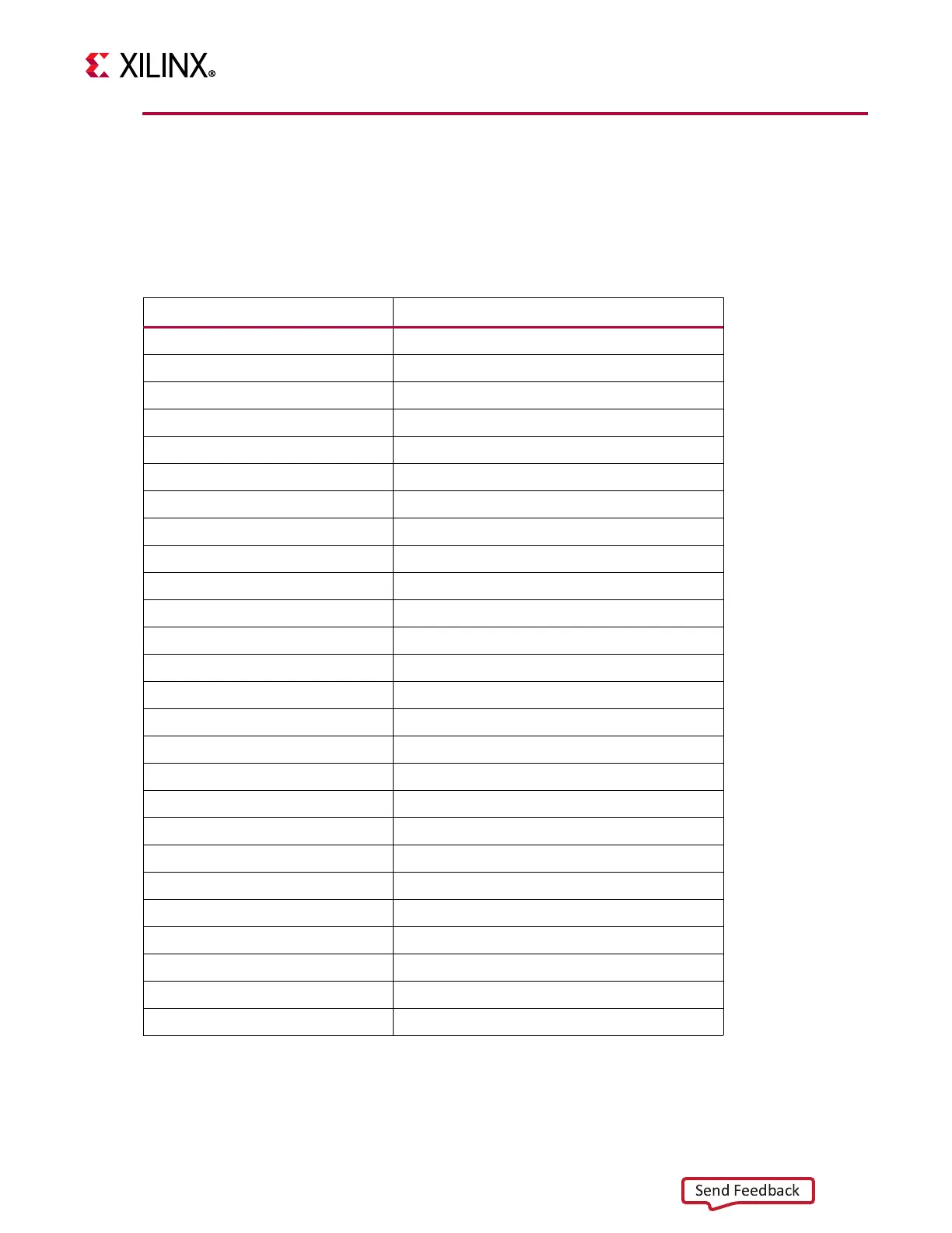
Table D-2: XM500 ADC/DAC Data and Clock Mapping
SMA Ref. Des. ADC/DAC Data or Clock
J26(P)/J27(N) DAC228_T0_Ch0
J20(P)/J21(N) DAC228_T0_Ch1
J22(P)/J23(N) DAC228_T0_Ch2
J24(P)/J25(N) DAC228_T0_Ch3
J7 DAC229_T1_Ch0
J8 DAC229_T1_Ch1
J5 DAC229_T1_Ch2
J6 DAC229_T1_Ch3
J4 ADC224_T0_Ch0
J3 ADC224_T0_Ch1
J2 ADC225_T1_Ch0
J1 ADC225_T1_Ch1
J33(P)/J32(N) ADC226_T2_Ch0
J34(P)/J35(N) ADC226_T2_Ch1
J37(P)/J36(N) ADC227_T3_Ch0
J39(P)/J40(N) ADC227_T3_Ch1
J30(P)/J31(N) ADC224_T0_CLKIN
J889(P)/J890(N) ADC225_T1_CLKIN
J891(P)/J892(N) ADC226_T2_CLKIN
J893(P)/J894(N) ADC227_T3_CLKIN
J28(P)/J29(N) DAC228_T0_CLKIN
J896(P)/J895(N) DAC229_T1_CLKIN
J898(P)/J897(N) DAC230_T2_CLKIN
J900(P)/J899(N) DAC231_T3_CLKIN
J9 2x10 header See Figure D-5
J10 2x10 header See Figure D-5

 Loading...


