ZCU111 Board User Guide 44
UG1271 (v1.1) August 6, 2018 www.xilinx.com
Chapter 3: Board Component Descriptions
The LED functions can be repurposed with a LEDCR1 register write available via the PHY's
management data interface, MDIO/MDC. LED_2 is assigned to ACT (activity indicator) and
LED_0 indicates link established. For more Ethernet PHY details, see the TI DP83867 data
sheet [Ref 20]. LED_1 (100BASE-T link established) is a separate LED DS27 located on the
top side of the board near the RJ45 P12 connector (Figure 2-1, callout 12).
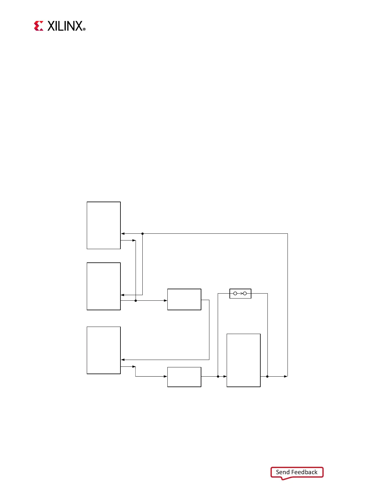
Programmable Logic JTAG Programming Options
[Figure 2-1, callouts 7 and 63]
ZCU111 JTAG chain:
• J83 USB micro AB connector connected to U34 FT4232HL USB-JTAG bridge
• J13 2x7 2 mm shrouded, keyed JTAG pod flat cable connector
The ZCU111 board JTAG chain is shown in Figure 3-12.
X-Ref Target - Figure 3-12
Figure 3-12: JTAG Chain Block Diagram
JTAG
2 mm 2X7
Header
J13
TDO
TDI
FT4232HL
UART
BRIDGE
U34
TDO
TDI
JTAG
IF
PS Config
Bank 503
U1
TDI
TDO
JTAG
TDI
BUF
U32
AB
U45
JTAG
TDO
BUF
U30
BA
FMCP HSPC
Connector
(D)
J26
TDI TDO
N.C.
X20535-062118

 Loading...


