ZCU111 Board User Guide 53
UG1271 (v1.1) August 6, 2018 www.xilinx.com
Chapter 3: Board Component Descriptions
RF Data Converters
The ZU28DRF-FFVG1517 contains eight multi-gigasample (4 GSPS), 12-bit RF
analog-to-digital converter (RF-ADC) channels across four banks and eight
multi-gigasample (6.544 GSPS), 14-bit RF digital-to-analog (RF-DAC) converter channels
across two banks. The ZCU111 board provides a pair of Samtec LPAF connectors (J47: ADC;
J94: DAC) for the RF-ADC/RF-DAC clock and RF signals.
RF Data Converter Clocking
The RF data converter clocking includes primary on-board reference PLL (LMK04208) and
on-board RF PLLs (LMX2594) to generate RF-ADC and RF-DAC sample clocks. With careful
board modification, external equipment can also directly drive ADC bank clocks and DAC
bank clocks through the Samtec LPAF (8x40) connector.
The LMX2594 clocks can be configured either as direct RF clocks or as reference clock
sources for the internal PLL contained within the RFSoC data converter tile.
See ZCU111 System Controller Tutorial (XTP517) [Ref 11] for information on programming
the LMK and LMX PLLs.
Two Samtec LPAF (8x40) connectors provide an RFMC system interface for plug-in cards.
Figure 3-20 and Figure 3-21 illustrate the connector pinout and plug-in card dimensions.
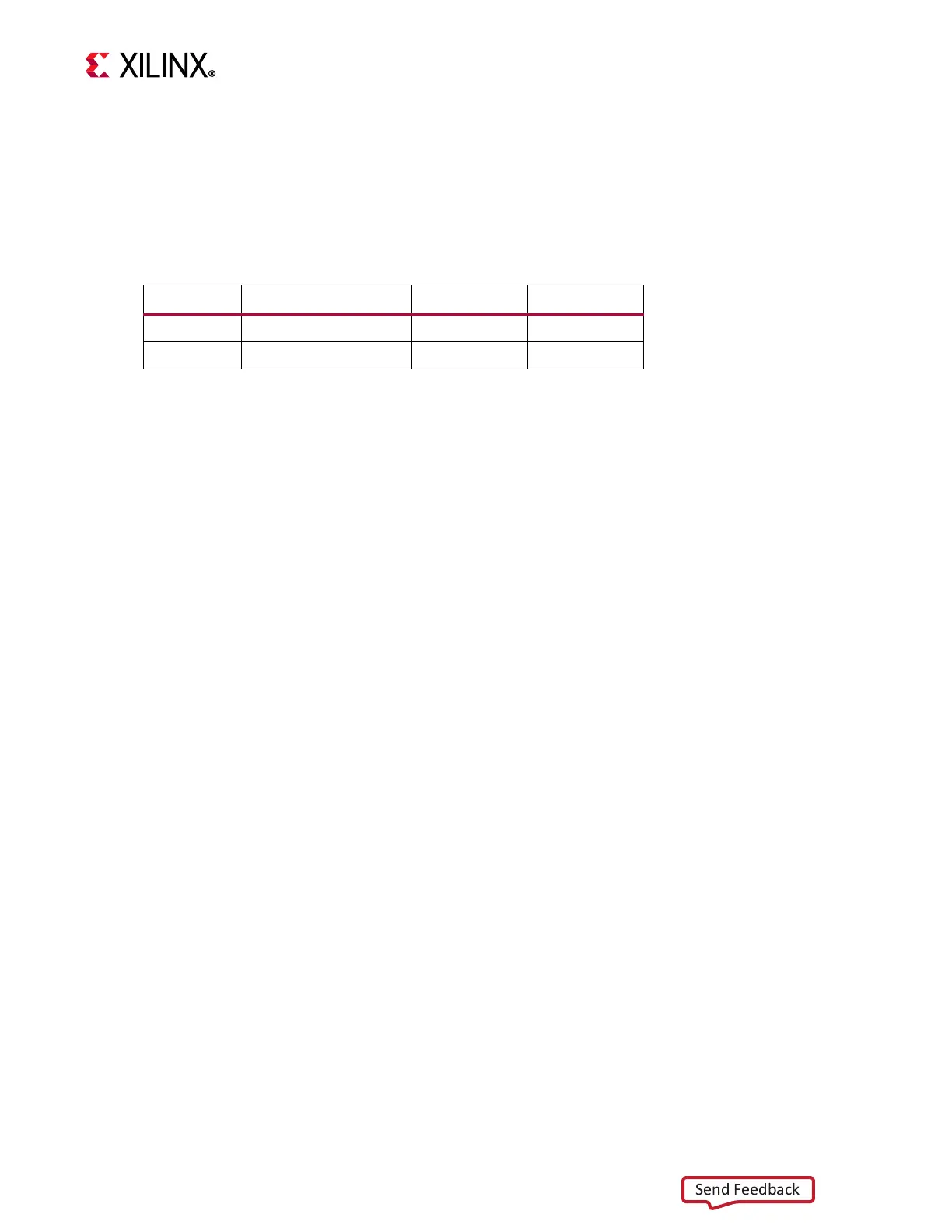
Channels per Bank Banks Channel Count
RF-ADC 2 4 (224-227) 8
RF-DAC 4 2 (228, 229) 8

 Loading...


