
Do you have a question about the Xilinx ZCU111 and is the answer not in the manual?
| Manufacturer | Xilinx |
|---|---|
| Model | ZCU111 |
| Form Factor | ATX |
| Processor | Quad-core ARM Cortex-A53 |
| FPGA | Xilinx Zynq UltraScale+ RFSoC |
| Memory | 4GB DDR4 |
| Power Supply | 12V DC input |
| Storage | microSD slot |
| Connectivity | Gigabit Ethernet, USB 3.0, USB 2.0 |
| Expansion | FMC |
| RFSoC | Yes |
Provides a general overview of the ZCU111 evaluation board and its features.
Lists additional documents and resources relevant to the ZCU111 evaluation board.
Illustrates the ZCU111 evaluation board's block diagram for component interconnection.
Details the key features and specifications of the ZCU111 evaluation board.
Covers physical dimensions, environmental operating conditions, and voltage requirements.
Details the physical locations of components on the ZCU111 evaluation board.
Provides default jumper and switch settings for board configuration.
Explains configuration options for the RFSoC device booting process.
Detailed description of the Zynq UltraScale+ XCZU28DR RFSoC device on the board.
Describes the circuit for backing up the encryption key using a battery.
Details the PS-side and PL-side DDR4 memory configurations.
Explains the PSMIO peripheral mapping for the ZCU111 board.
Describes Quad SPI Flash memory and GPIO connections.
Details the I2C0 and I2C1 bus connectivity and multiplexer configurations.
Explains the UART0 interface and its connection to the FTDI chip.
Covers USB 3.0 Transceiver and USB 2.0 ULPI PHY functionality.
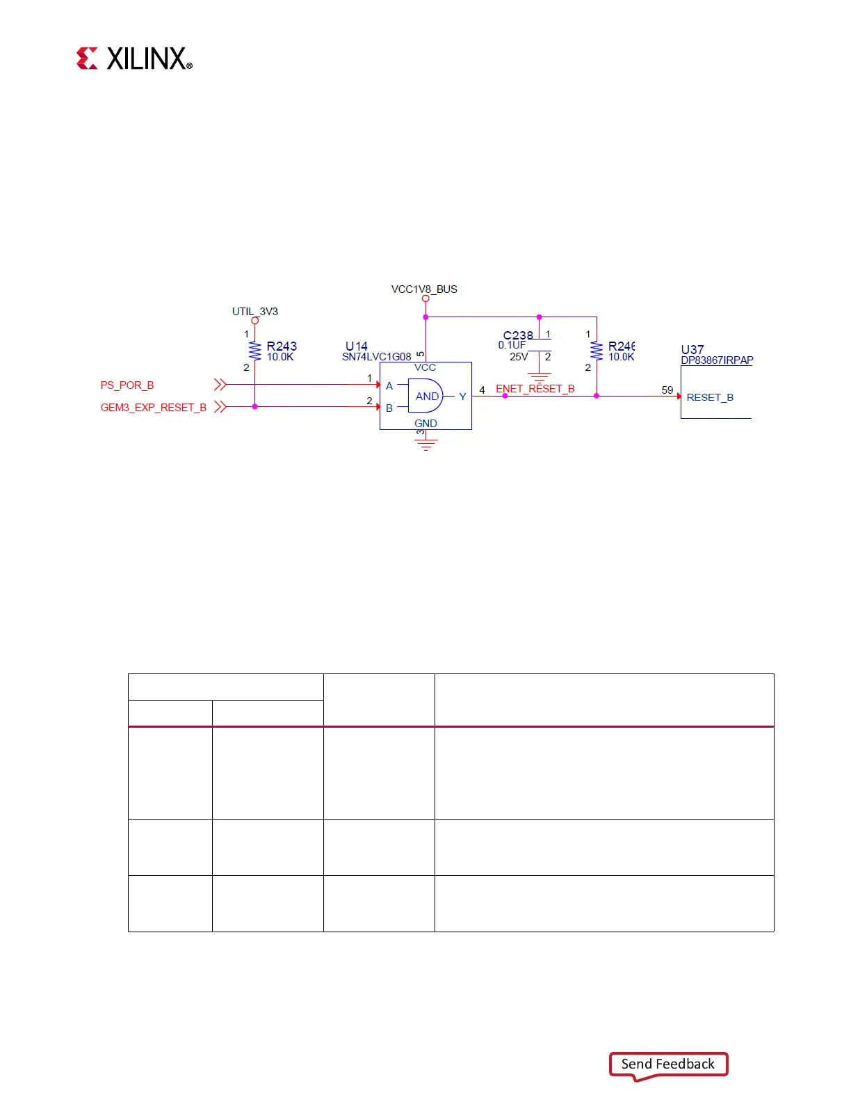
Details the GEM3 Ethernet and 10/100/1000 MHz Tri-Speed Ethernet PHY.
Explains the options for programmable logic JTAG programming.
Describes clock sources, including fixed, programmable, and SMA clocks.
Details the four SFP28 connectors and their associated circuitry.
Describes the two PMOD GPIO receptacles for user connections.
Details user-controlled I/O capabilities: LEDs, DIP switches, and pushbuttons.
Defines the functionality of the power and status LEDs on the board.
Covers GTY and GTR transceivers, including their bank assignments and connectivity.
Describes the M.2 SATA interface for accessing SATA SSDs.
Explains the VITA 57.4 FMC+ specification and the ZCU111's implementation.
Details the cooling fan connector and its autonomous speed control.
Describes the on-board system controller and its user interface (SCUI).
Details the power management ICs and regulators used on the board.
Explains how to monitor voltage and current using Infineon power controllers.
Shows the pinout of the FMCP high pin count connector defined by VITA 57.4.
Provides information on Xilinx design constraints (XDC) for the ZCU111 board.
Details conformity to European Union directives and standards.
Lists relevant CE directives for Low Voltage and EMC.
Defines CE standards from CENELEC and IEC.
Specifies limits and methods for IT equipment radio disturbance and immunity.
Lists safety standards for information technology equipment.
Explains product compliance markings like WEEE, RoHS, and CE.
Introduces the FMC-XM500 RFMC plug-in card for ADC/DAC clocking and RF signals.
Describes the Samtec LPAM connectors on the XM500 card for interface access.
Lists the components and their locations on the XM500 card.
Details the mapping of ADC/DAC bank data and clock channels.
Provides details on XM500 ADC/DAC data and clock SMA connections.
Lists support resources available from Xilinx.
Provides information on Xilinx Solution Centers for device and software support.
Explains how to access Xilinx documents, videos, and support resources.
Lists websites and documents for supplemental material.
Contains important legal notices and disclaimers regarding product usage.


