3 - 26
MELSEC-Q
3 SPECIFICATIONS AND FUNCTIONS
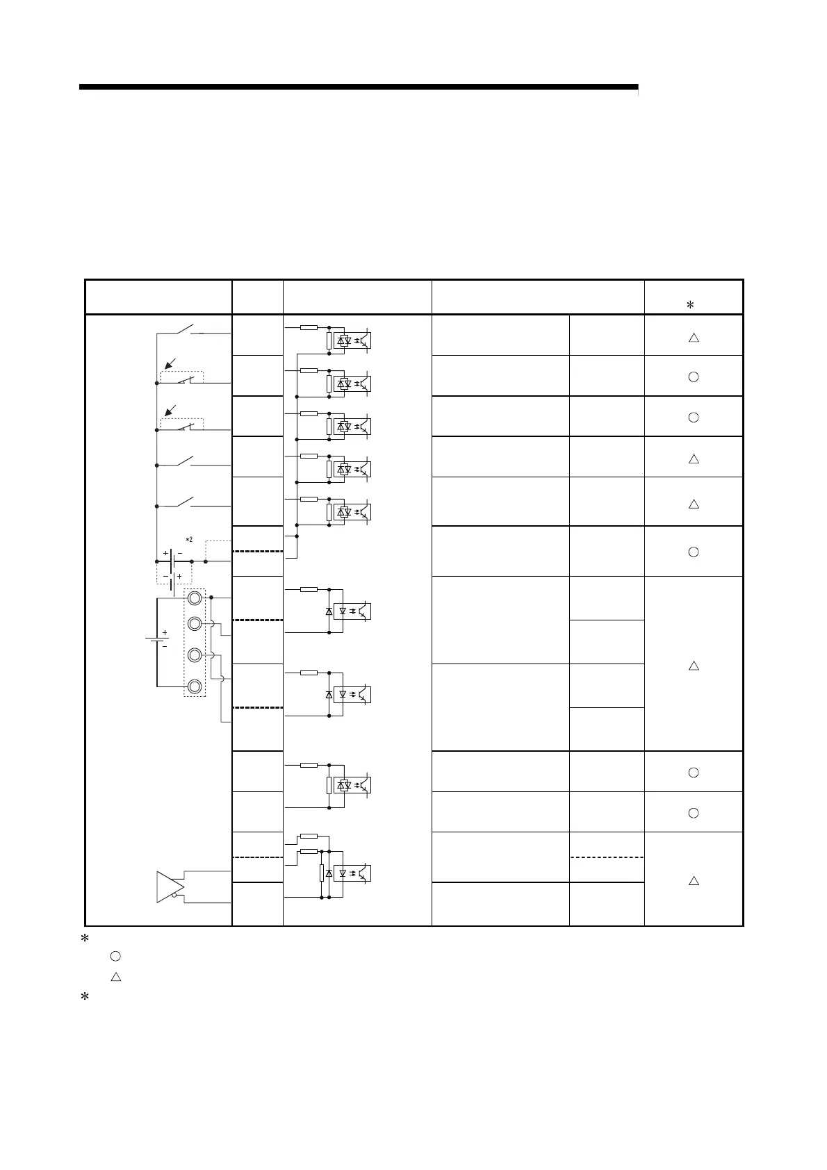
3.4.4 Input/output interface internal circuit
The outline diagrams of the internal circuits for the
QD75P1N/QD75D1N/QD75P1/QD75D1 external device connection interface are
shown below.
(1) Input (Common to QD75P1N, QD75D1N, QD75P1, and QD75D1)
External wiring Pin No. Internal circuit Signal name
Need for wiring
1
1A3
Near-point dog signal DOG
1A1
Upper limit signal FLS
1A2
Lower limit signal RLS
1A4
Stop signal STOP
1A5
External command
signal
CHG
1A6
1A7
Common COM
(+)
1A19
PULSER A+
(–)
1B19
Manual pulse generator
A phase
PULSER A–
(+)
1A20
PULSER B+
(–)
1B20
Manual pulse generator
B phase
PULSER B–
1A11
Drive unit READY READY
1A12
Drive unit READY
common
RDY COM
1A8 PG024
1A9
Zero signal
PG05
5VDC
5V
0V
A
B
24VDC
When upper
limit switch is
not used
When lower
limit switch is
not used
Manual pulse
generator
(MR-HDP01)
1A10
Zero signal common PG0 COM
1: The symbols in Need for wiring column indicate the following meanings:
• : Wiring is necessary for positioning.
• : Wiring is necessary depending on the situation.
2: Either polarity can be connected to the common (COM).
 Loading...