11-4
Specifications Section 1-2
BCD
Communications
Note (1) Common pins 1, 25, and 37 are internally connected.
(2) Pin 29 is the HOLD input to the K3HB-X/V/H/S/R/P, and the COMPEN-
SATION input to the K3HB-C.
(3) OUT1 to OUT5 are for the K3HB-C.
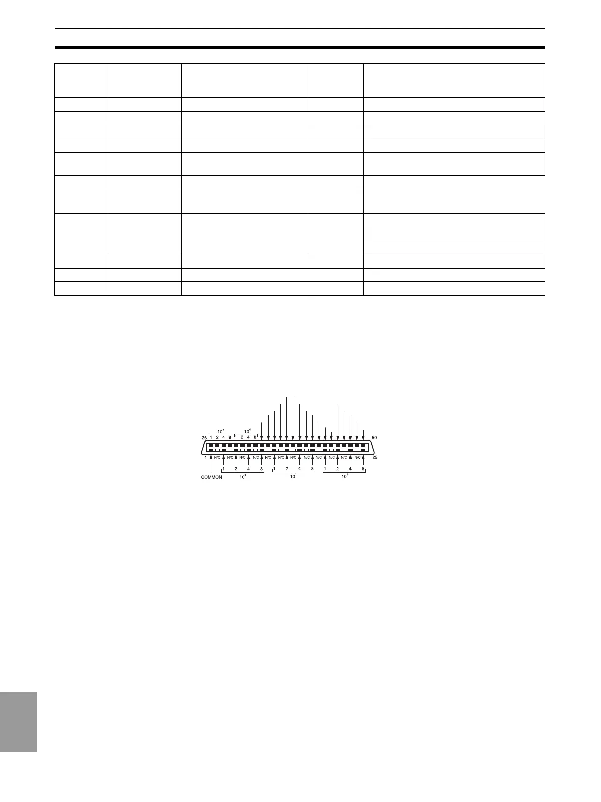
1-2-3 Pin Wiring Diagram
Note (1) Either of the BCD common pins can be used for any of the signals.
(2) Pins shown as blank in the diagram (@) have been removed.
(3) OUT1 to OUT3 and COMPENSATION are for the K3HB-C.
• Applicable connector (sold separately): HDR-E50MAG1 (made by Honda
Tsushin Kogyo Co., Ltd.)
• Special cable (sold separately): K32-BCD (OMRON), (HDR-E50MAG1
and 0.3-m cable)
25 37 COM
26 38 REQ Input Measurement value output request
27 39 MAX Input Maximum value output request
28 40 MIN Input Minimum value output request
29 41 HOLD (COMPENSATION) Input HOLD input (COMPENSATION input)
See note 2.
30 42 RESET Input RESET input
31 43 POL Output Data polarity signal (− when ON, + when
OFF)
32 44 HH (OUT5) Output Output HH (OUT5) See note 3.
33 45 H (OUT4) Output Output H (OUT4) See note 3.
34 46 PASS (OUT3) Output Output PASS (OUT3) See note 3.
35 47 L (OUT2) Output Output L (OUT2) See note 3.
36 48 LL (OUT1) Output Output LL (OUT1) See note 3.
37 49 COM GND: V0
K32-BCD
pin
number
Digital
Indicator BCD
pin number
Signal name Signal
direction
Meaning
OVER
DATA VALID
RUN
COMMON
REQUEST MAX REQ.
MIN REQ.
RESET
POLARITY
HH(OUT5)
H(OUT4)
COMMON
N/C
HOLD(COMPENSATION)
PASS(OUT3)
L(OUT2)
LL(OUT1)
 Loading...