EasyManua.ls Logo

Renesas TPS-1 User Manual

Renesas TPS-1
91 pages
To Next Page IconTo Next Page
To Previous Page IconTo Previous Page
Page #26 background imageLoading...
Page #26 background image
TPS-1 Users Manual: Hardware 3. Host Interface
R19UH0081ED0107 Rev. 1.07 page 26 of 86
Jul 30, 2018
3.3.1.2. Structure of a command byte
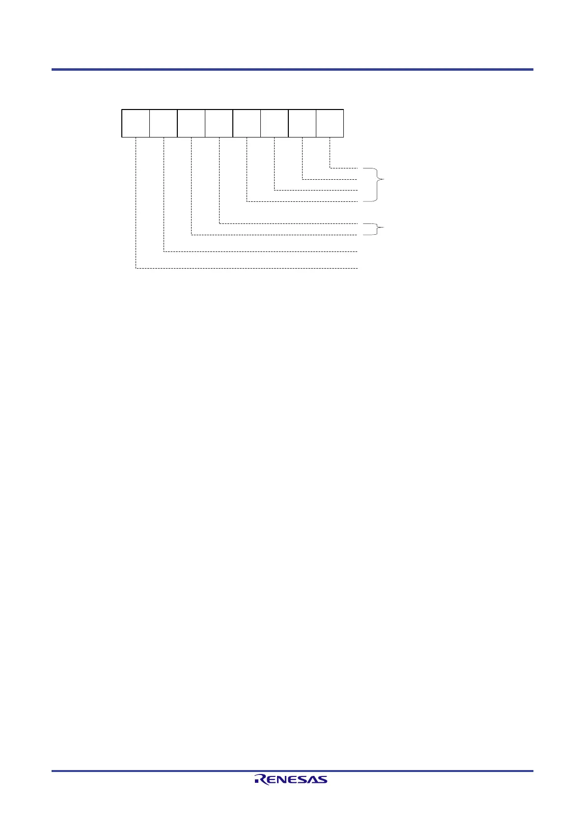
Figure 3-9 shows the format of a command byte. A command byte can be followed by an address area, length area and data.
b7 b6
b
5 b
4
b3
b2
b
1 b0
Access Area
Direct IO Length
b6 = 1 (write)
b7 = 1 (read)
Figure 3-9: Command byte for SPI slaves (host interface)
The bits of the command byte have the following meaning:
b7 indicates a read command,
b6 indicates a write command,
b5 and b4 describe the addressing range:
„00“: MEM access to the complete shared memory (64 Kbyte)
„01“: IO access to the input/output area
„10“: access to a multicast provider CR (only write)
„11“: fractional access to an I-CR (b6 = 1) or MC-CR (b6 = 0)
b3 .. b0 contain the length for an optimized direct data access
„= 0000“: no direct access.
0000“: direct access length information (maximum of 15 byte)

Table of Contents

Question and Answer IconNeed help?

Do you have a question about the Renesas TPS-1 and is the answer not in the manual?

Renesas TPS-1 Specifications

General IconGeneral
ModelTPS-1
Communication InterfacesEthernet, SPI, I2C
Operating Voltage3.3 V
CategoryController
ManufacturerRenesas
CompliancePROFINET
InterfaceEthernet
Supply Voltage3.3 V
Operating Temperature-40°C to 85°C
PackageLQFP

Summary

Notice

Instructions for the Use of Product

How to Use This Manual

List of Abbreviations and Acronyms

Overview

1.1 Features

Detailed list of the PROFINET Device Chip TPS-1's capabilities and functionalities.

1.2 Abstract

Concise summary of the TPS-1 chip's purpose and integration for PROFINET automation.

1.3 Block Diagram

Visual representation of the TPS-1's internal structure and main components.

Pin Function

2.1 Signal Overview and Description

Comprehensive details on each signal pin of the TPS-1 and its designated function.

2.2 GPIO Multiplexing

Mapping and alternate functions of the 48 General Purpose Input/Output pins.

2.3 Supply Voltage Circuitry

Specifies the required supply voltages and their generation for the TPS-1's operation.

2.4 Signals for IRT Communication

Details synchronization trigger signals used for PROFINET IRT communication.

Host Interface

3.1 Testing DPRAM Interface

Information on testing the DPRAM interface with specific address values.

3.2 Parallel Interface

Configuration and signal details for connecting a host CPU via the parallel interface.

3.3 SPI Slave Interface

Setup and timing information for connecting a host CPU using the SPI slave interface.

Shared Memory Structure

4.1 Event Communication with the TPS-1 Firmware

Explains how the TPS-1 and host CPU exchange events via registers.

4.2 Events from the TPS-1 Firmware to the Host

Lists events generated by the TPS-1 firmware sent to the host CPU.

4.3 Events from the Host to the TPS-1 Firmware

Lists events generated by the host CPU sent to the TPS-1 firmware.

4.4 Interrupt Communication with the TPS-1

Details on setting up and managing interrupt communication between TPS-1 and host CPU.

TPS-1 Boot Subsystem

5.1 Hardware Structure for the Boot Operation

Overview of the hardware architecture supporting the TPS-1's boot process.

5.2 Loading and Update of the Firmware

Procedures for loading and updating the device firmware during manufacturing.

5.2.2 SPI Master Interface (Boot Flash)

Details on the SPI master interface for connecting to the boot flash memory.

IO Local GPIO Interface

6.1 GPIO (Digital Input and Output)

Configuration and usage of the 48 General Purpose Input/Output pins.

6.2 Status LEDs of the TPS-1

Description of status LEDs connected to GPIOs for indicating device status.

6.3 I2C-Bus – LWL Diagnostic

Utilizing I2C interface lines for fiber optic diagnostic purposes.

TPS-1 Watchdog

7.1 Signal WD_OUT (Pin B12)

Details on the watchdog output signal indicating internal TPS-1 watchdog status.

7.2 Signal WD_IN (Pin A11)

Information on the watchdog input signal used for host CPU supervision.

PROFINET IO Switch

8.1 100Base-TX Interface

Physical transmission and signal line details for the 100Base-TX Ethernet interface.

8.2 100Base-FX Interface (Fiber Optic)

Specifications and connection details for the 100Base-FX fiber optic Ethernet interface.

8.3 I2C-Bus – LWC Diagnostic

Using I2C interface lines for fiber optic diagnostic purposes.

8.5 Integrated Voltage Regulator 1.5 V

Details on the internal 1.5V voltage regulator and its operation.

Clock Circuit

9.1 Using the Internal Clock Oscillator

Guidance on using an external oscillator for the TPS-1's clock distribution.

9.2 External Clock Source

Parameters and requirements for using an external clock source for XCLK1.

Reset of the TPS-1

Boundary Scan Interface (JTAG)

11.1 Circuit Recommendation of the JTAG Interface

Recommended circuit configurations for the JTAG interface for various use cases.

Appendix A: Setting of Operating Modes

A.1 Host Interface

Configuration options for host CPU connection via serial or parallel interfaces.

A.2 Local I/O-Configuration

Settings for GPIO control and SPI master interface for local IO devices.

A.3 Ethernet Interface Configuration

Configuration of IP addresses, MAC addresses, and serial number for Ethernet communication.

A.4 Copying the Configuration Data into the Boot Flash

Procedure for transferring configuration data to the PROFINET device's boot flash.

A.5 Generating a Complete Serial Boot Flash Image

Steps to create a complete boot flash image for the TPS-1 device.

Appendix B: Board Design Information

B.1 Voltage Supply

Required supply voltages and their delivery methods for the TPS-1.

B.2 Switching Regulator

Details and wiring recommendations for the integrated 1.5V switching regulator.

B.3 Board Design Recommendations for Ethernet PHY

Guidelines for designing the PCB circuitry for Ethernet PHY components.

Appendix C: Fast Start Up Requirements