Mounting and Commissioning
3.1 Mounting and Connections
SIPROTEC, 7SD610, Manual
C53000-G1176-C145-6, Release date 02.2011
277
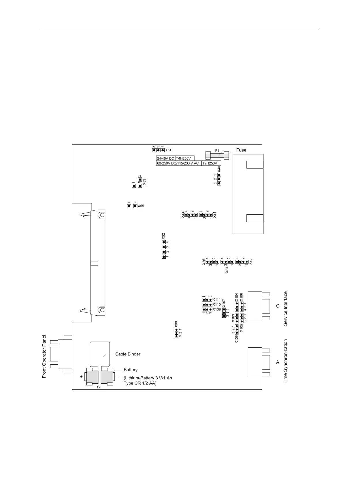
3.1.2.3 Switching Elements on Printed Circuit Boards
C-CPU-2 processor board
The PCB layout of the processor board C–CPU-2 is illustrated in the following figure. The set nominal voltage
of the integrated power supply is checked according to Table 3-2, the quiescent state of the life contact accord-
ing to Table 3-3, the selected control voltages of the binary inputs BI1 to BI5 according to Table 3-4 and the
integrated RS232 / RS485 interface according to Table 3-5 to 3-7. The location and ratings of the miniature fuse
(F1) and of the buffer battery (G1) are shown in the following figure.
Before checking the integrated RS232/RS485 interface it may be necessary to remove the interface modules
placed above.
Figure 3-4 Processor printed circuit board C-CPU-2 with jumpers settings required for the board configuration
 Loading...