(BVM-1911 ONLY)
3-8. NTSC COMB FILTER (BT BOARD)
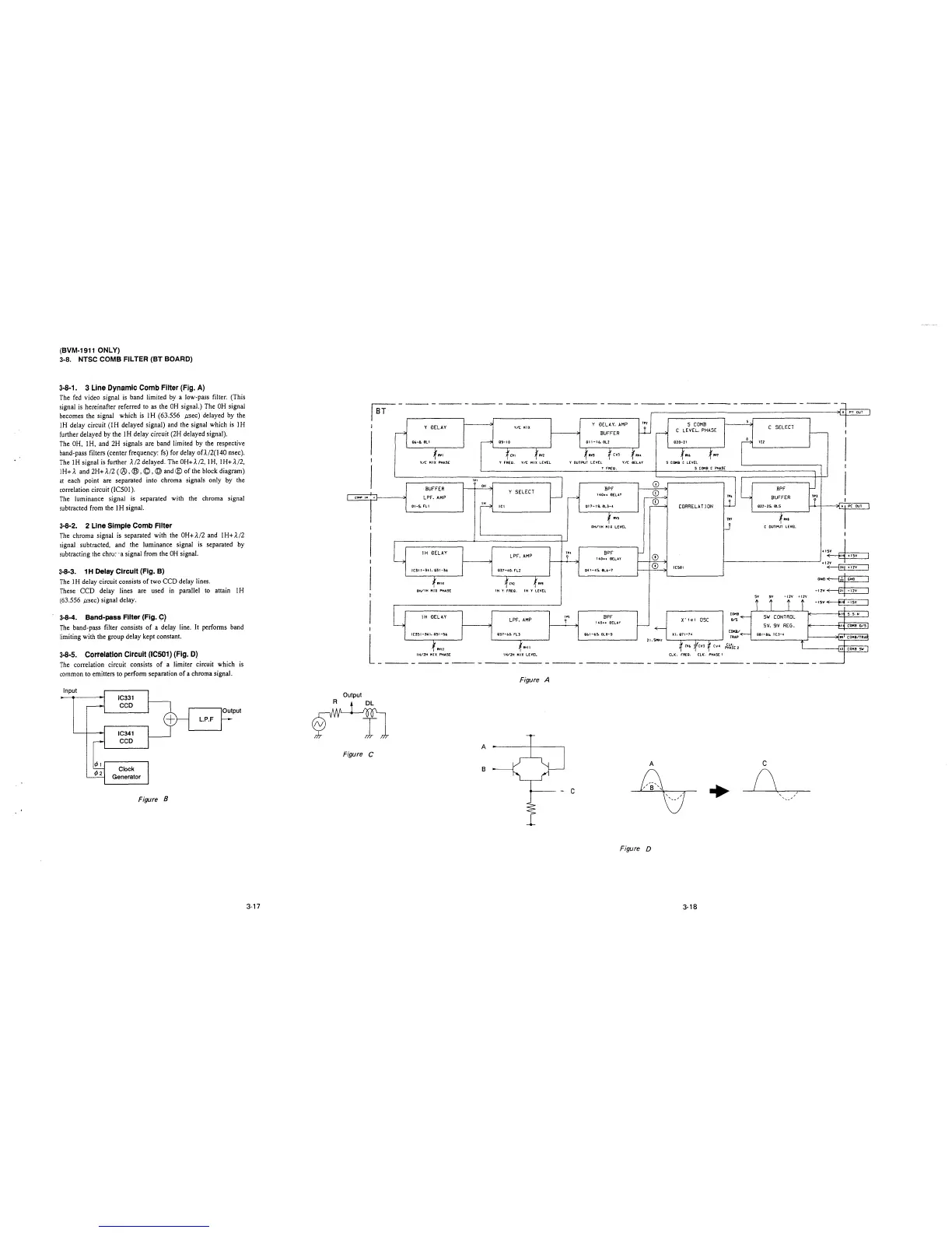
3-8-1. 3 Line Dynamic Comb Filter (Fig. A)
The fed video signal is band limited by a low-pass filter. (This
signal is hereinafter referred to as the OH signal.) The OH signal
becomes the signal which is 1H (63.556 µ.sec) delayed by the
1H delay circuit (IH delayed signal) and the signal which is 1H
further delayed by the 1H delay circuit (2H delayed signal).
The OH, IH, and 2H signals are band limited by the respective
band-pass filters (center frequency: fs) for delay of.A./2(140 nsec).
The 1 H signal is further A /2 delayed. The OH+ A /2, 1 H, 1 H+ A /2,
lH+ A and 2H+ A/2 ( ®,®,©,@and® of the block diagram)
at each point are separated into chroma signals only by the
correlation circuit (IC501 ).
The luminance signal is separated with the chroma signal
subtracted from the IH signal.
3-8-2. 2 Line Simple Comb FIiter
The chroma signal is separated with the OH+ A/2 and IH+ A/2
signal subtracted, and the luminance signal is separated by
subtracting the chro~ · a signal from the OH signal.
3-8-3. 1 H Delay Circuit (Fig. B)
The IH delay circuit consists of two CCD delay lines.
These CCD delay lines are used in parallel to attain IH
(63.556 µ.sec) signal delay.
3-8-4. Band-pass Filter (Fig. C)
The band-pass filter consists of a delay line. It performs band
limiting with the group delay kept constant.
3-8-5. Correlation Circuit (IC501) (Fig. D)
The correlation circuit consists of a limiter circuit which is
common to emitters to perform separation of a chroma signal.
Input
IC331
CCD
IC341
CCD
Clock
Generator
Figure 8
L.P.F
3-17
rsr----------------------------
lIJ I PY OU1
I
-
Y DELAY. AMP
'
S COMB
5
I
Y DELAY
Y/C HIX
C SELECT
I
r-o,
BUFFER
r-o,
C LEVEL PHASE
,___
I
,
06-& DL I
r--i'
09-10
011-16. OL2
020-21
~
IC2
I
f .. ,
f CYI
fm
f ...
f CV5
t ...
f .. ,
1 ...
I
Y/C HIX PHA.5(
Y FREQ. Y/C HIX LEVEL Y OUTPUT LEVEL Y/C OELAY S CONS C LEVEL
I
Y FREQ. S COHB C PHASE
I
I
I
TPI
LJ
0
L
J
BUFFER
OH
BPF BPF
Y SELECT
©
r
COO<' , •
.
-
LPF. AMP
r-i'
140 .. DELAY
~
""
BUFFER
,.,
I
rl
-L
r
I
01-s. Flt
ICI
017-19. OL3-4
~
CORRELATJON
022-25. OLS
.._ 'I PC OUT
I
f RYS
m
f ...
I
I
DH/IH NIX LEVEL
_j
C OUTPUT LEVEL
I
I
L
IH DELAY
, ..
BPF
~
+I~
LPF. AMP
?
0
t • 15Y
I
140 .. DELAY
0
-ti 2V
I
JC31 l-341, 031-3&
037-40. f"L2
Q41-,s. DU,-7
1(501
~
f .. .,
~CYl
f ...
G~~
OH/IH NIX PHASE IH Y FREQ. IH Y LEVEL
-12Y 11 -12Y
!
t z
-12v
... ,.,.,
I
i f
-ISY~
L
I
IH DELAY
'"'
BPF
c:;,•-
5.,,, CONTROL
t~ S.S.N
I
LPF. AMP
?
140., OELAY
X" to I
DSC
I
-
I
~-
SV, 9V REG.
I~ COKB 11/5 I
JC35J-3l:.I. 051-51:. 057-60. F'L! Q6 l -6S. OL8-9 XI. 071-74
COKll/-<i--
CIS 1-86. I C3-4
TRA.P
19 CONB/TRA~
f IIVIZ
f IIYII
21. 5HH1
~
CY6 fmf CV'
i
cue.
PHASE 2
u COl'lB 51{ I
l ow> "" -• ow• "" um "'· ,oo. "' -",
-------------------------------------------------------~
Figure A
Output
A
Figure C
A C
B
.,, ... 9,,,
•
(\
'
,
'
,
,
'
,
'
,
'
,
Figure D
3-18
 Loading...