3-16. HIGH VOLTAGE REGULATOR (PA BOARD)
This high voltage regulator uses also DC-DC converter so as to
reduce power consumption.
The theory of operation of this circuit is as follows.
3-16-1. Detection of High Voltage
High Voltage applied to the CRT anode is converted to the low
voltage by OCT block (Dynamic Convergence Transformer). This
low voltage is fed to buffer amplifier IC4(2/2) and compared with
external reference voltage in !Cl. The DCT contains resistor-
network and transformer for conver!!ence adjustment. This resistor-
network works as a voltage divider.
3-16-2. PWM Modulator
[Cl works as error amplifier and PWM modulator comparing volt-
age between high voltage and the reference voltage is amplified
and modulated so as to drive QJ02 output transistor. Output
signal from !Cl, which is modulated in PWM, is fed to Ql02 via
drive transformer. +B line supplied to I BT ( Fly Back Transformer)
circuit is controlled by switching Ql02 output transistor on/off.
3-16-3. Output Circuit
When high voltage drops down, output voltage of DCT also drops
as above mentioned. At this time PWM circuit is designed so that the
ON period of Ql02 output transistor should be longer than high
voltage drops down. +B line, switchied ON/OFF by Ql02, is sup-
plied to converter circuit which drives FBT via LOT (Line Output
Transformer).
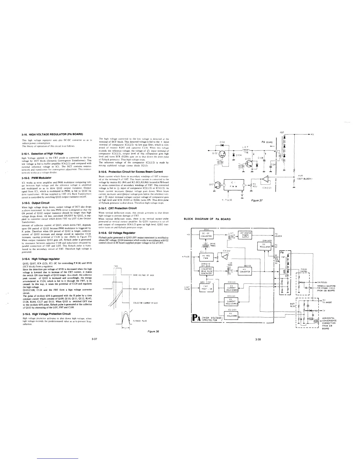
Amount of collector current of Ql03, which drives FBT, depends
upon ON period of QI02 because PWM modulator is triggered by
H. pulse. Therefore when ON period of Ql02 is longer, collector
current of Ql03 increases and energy stored in capacitor Cl 24
Increases, causing potential of Cl24 to rise. (Refer to Figure 37)
When output transistor Ql03 goes off, flyback pulse is generated
by resonance between capacitor CI 08 and inductance obtained by
parallel connection of FBT and LOT. This flyback pulse is trans-
ferred to the secondary circuit of FBT. Therefore high voltage is
generated.
3-16-4. High Voltage regulator
Ql02, Ql07, IC4 (2/2), IC! (IC for controlling P.W.M) and HVR
(DCT block) form a regulator.
Since the detection pin voltage of HVR is decreased when the high
voltage is lowered due to increase of the CRT current, it makes
the switch ON time length ofQ!02 longer. As a result, the collector
peak cun-ent of Ql 03 is increased and accordingly, the energy
accumulated in Cl24, which is fed to it through the FBT, is in-
creased. In this way, it raises the potential of Cl 24 and regulates
the high voltage.
Ql 03,Cl 08, C124 and the FBT form a hign voltage converter
circuit.
The pulse of on-duty 60% is generated with the H pulse by a time
constant circuit which consists ofQ109, QllO, Ql11, Ql12, Rl43,
Cl 28, Rl44, Cl27 and D111. When Q103 is switched OFF due
to the on-duty 60% pulse, flyback pulse is generated at the collector
of Ql 03 by resonating of the LOT, FBT and Cl 08.
3-16-5. High Voltage Protection Circuit
High voltage protector activates to shut down high volta!!e, when
high volta!!e exceeds the predetermined value so as to prevent Xray
radiation.
3-37
The high voltage converted to the low voltage is detected at the
terminal of DCT block. This detected voltage is fed to the + input
terminal of comparator IC2(2/2) via low pass filter, which is com-
posed of resistor R245 and capacitor C2 ! 6. When this vo!tage
exceeds the reference voltage, the voltage of 0 input terminal of
comparator IC2(2/2), output level of this comparator goes high
level and turns SCR (0206) gate on to shut down the drive rulse
of flyback !!enerator. Thus high volta!!e stops.
The reference voltage of the comparator IC2(2/2) is made by
mixin!! stabilized volta!!e (Zener diode D215)
3-16-6. Protection Circuit for Excess Beam Current
Beam current which t1ows in secondary windings of I· l:lT is measur-
ed at the terminal 9 of 1-1:lT. This beam current is converted to the
voltage by resistor RI (R4) and R2 (R3), RS(R6) located in PB board
in, series connection of secondary windings of FBT. This converted
voltage is fed to e input of comparator IC2(1/2) or IC3(1/2). As
beam current increases. 0input voltage goes down. When beam
current increases until 0input volta!!e goes below the reference volt-
age ( 0 input terminal volta!!e) output voltage of comparator goes
up high level and SCR (D205 or D206) turns ON. Thus drive pulse
of tlyback generator is shut down. Therefore hi!!h volta!!e stops.
3-16-7. CRT Protection Circuit
When vertical deflection stops. this circuit activates to shut down
hi!!h voltage to prevent damage of CRT
When vertical deflection stops, there is no vertical output pulse
generated at vertical output amplifier. So 0201 transistor is cut off
and output of comparator IC4(1/2) goes up high leveL Q202 tran-
sistor turns on and t1yback )lenerator -tops.
3-16-8. G2 Voltage Regulator
Flyback pulse generated at Q103 (HY output transistor) is rectified to
obtain DC voltage. Q104 transistor which works in accordance with G2
control circuit in BI board supplied proper voltage to G2 of CRT.
:'l___
' I
____ ,_,'
,
,
/
I
I
I
I
J1
,-\'.
h~
BASE VOLTAGE OF 0102
BASE VOLTAGE OF 0103
COLL EC TOR CURRENT OF 0103
FLYBACK PULSE
Figure 36
0102
L O T
0102
-
D 10 4
r+,-
Q 103
~11/
IC I
P W M
H. PULSE
BLOCK DIAGRAM OF PA BOARD
0102
t B I>----' DC - DC
CONVERTER
H. PULSE o-...-~
v.ouT 1,.... _ __._,
PULSE
__\,gJ_ DRIVE
~
TRAN S
IC I
HV REG
PWM
0109.0110
0 II I O I 12
CONVERTER
DRIVE PULSE
GENE RA TOR
1(412/2!
I C2 I I/ 2 I
H V
CURRENT
HOLD DOWNII
IC 3 I 1/ 21
HV
CURRENT
HOLD DOWNl2
Ic212121
HV
CRT HEATER
POWER
SUPPLY
0 I 03
HV
CONVERTER
FBT
r------------HV
PA
BOARD
CI08
I
(124
I
HV
ADJ
I (412/21
Figure 37
TO
t---------HEATER
0104 0105
G2
REGULATOR
TO
G2
G2
I
I
,+,-
B
CONT- T
ROL
I FROMi
181
-
H VR
( OCT BLOCK )
FOCUS
CONTROL
r - -- -,
I I
I I
~Vw--<:>--!---o,. G 4 I FOCUS)
I
PARABOLA WAVEFORM
1--<'.>4+--FOR OYNAMI C FOCUS
I I
FROM EB BOARD
L ____ .J
r--,--.--.__--0-- ... HV
OCT
1
BLOCK I
I
TO ANODE
HOLD DOWN ,__ ____________ e,_ __ ----.J
3-38
 Loading...