(BVM-1911 ONLY)
3-10. NTSC DEMODULATOR, Y TRAP CIRCUIT
(BC BOARD)
l he comrositc video signal ( NTSC) ,upplied from BA board is
fed to transistor Ql (buffer). then is supplied to the 3.58MHz
trap cm:uit with Y siµnal and to hand pass filter \\ith chrominance
,ignal.
3-10-1. Chroma Band Pass Filter
The composite video signal obtained from at the emitter of tran·
sistor QI is fed to the Band pass filter composed of resistor RI 8.
capacitor C7. C8. inductor L3 and transistor QS.
fhe center frequency of this tilter is adjusted to the subcarrier
lrcquenc, (3 58\,IH~) by L3. and chrominance signal is derived
lrom Q5.
This circuit selects comb filter (BB board) mode or notch filter
mode by a push of button on the front panel. When comb filter
mode is selected. comb switch circuit composed of transistor 0103
and Ql 04 activates and base volta!!e of QS goes down to - l 2V
and Ql 5 is cut off and then chrominance signal (Pure Cl is provided
frolT' comb filter circuit to 1C2.
3-10-2. Residual SW Circuit
The chrominance signal derived at transistor QS is fed to analog
switcher IC2 (Pin (2)).
When S\\Jtch SI on BJ h,1ard is set to ON position. residual pulse
"hic·h has almost same phase as II svnc 1s kd t<> control terminal
of analog switcher (pin 'J) of 1C2) and screening is performed
during H sync period.
When s\\ itch SI on BJ hoard is set to 011 posi1ion. Low level si~nal
10V DCI is fed to rnntrol terminal and screenin~ action 1s not rer-
lormed. Thus residual switch crrrnit does not activate.
When there is residual suhcamcr rn the video signal. damp level <>f
color difference signal c·han~es by turnrn~ S\VJtc·h Sl ON/O1·1 and
therefore residual suhcarricr can be checked on the picture as a
c·o!,,r shift.
J
~
t
H Sync
Color Burst
Figure 15
3-10-3. Chroma Amplifier Circuit
The level of chrominance siµnal from re,idual switch circuit I IC2
pin 3) ) is divided by resistor R85 and R86 and is fed to chroma
amplifier circuit 106. 07. 08).
The pin of this amplifier is almost I and this amplifier has 2
outputs. They are non-inverted signal and inverted signal.
Non-inverted signal is fed to R-Y input terminal ( IC 1 pin (3) ) of
demodulator and inverted si!!nal to B·Y input terminal ((Cl pinG)).
3-10-4. Phasa Control Circuit
The chrominance sif!nal from residual switch is also fed to phase
contrl circuit (09, 010, QI I, 012, D2).
In this circuit. a variable capacitance diode ( D2) is used to control
the phase of color burst signal.
Anode volta)!e of D2 is applied by variable resistor RV2 and preset
adJu'1ment of phase 1s made by this variahle resistor.
3-21
When the PHASE control on the ri)!ht side of the front panel is
turned. DC level of phase conttol si.enal ( board terminal A 13)
cl1an1?es and this phase control signal is fed to the cathode of D2
via analog switcher ([C2 PinG)l. In this way, Burst phase of chrorni-
nance signal is controlled according to the DC level of the phase
ontrol signal.
Analo,e switcher 1C3 ( 2/3) activates to make short-circuit between
input terminal pin @ and output terminal pin @ . only when
COLOR STANDARD SELECTOR in the right side of drawer is
selected to NTSC and otherwise pin @ kept opn circuit.
As above phase controlled chrominance si?nal is derived from
emitter of transistor QI 2 and burst signal in this signal
1
s gated bv
IC3 (1/3). The gated burst signal is fed to the bursi input ·termina.l
pin Cf]) of demodulator !Cl.
3-10-5. NTSC Demodulator
Block diagram of !Cl used for NTSC demodulator is shown in
Figure 16.
This lC i, desi~ned for u,e of NTSC dcnwdulator
When chrominance signal is fed to pin(D,G) and pin G), color burst
signal to pin _Cf]) and Burst Cate Pulse (B C.P) to pin Ci]). R-Y and
B-1 u,!or __ d1tterenc-e st~nals are <>htained at nutrut termin:ils rin ('_},
and pin ;'_4' ·
The demodulation asc·s of this denwdulatnr are R-Y asi, anrl B-Y
a\ls. Variahil' caracitor CV I is adjusted so that the phase an)!ie,
between them arc 90
Local oscillator (3 58MHz) is formed by CW oscillator in !Cl
connected to the terminal pin.]). C&_;, . <H .' and e, ternal circuit.
The variahle caracitor CV2 is ad1usted so that the free run frequen-
cy may be subcarrer trequency 3.579545"1Hz
Also APC IAut,Hnatic Phase Contrnl) c·ircu1t is formed h, APC
section in lC 1 connected to the terminal pin and local oscil-
lator is controlled by APC circuit.
The n>lor diffc·rc·nc·c· sl!!nal, demndula ted hy this IC .1re ted tu lll\s
pass filtl'f. \\here h1~h frequc'Jll') c·n111p,1n,·nt is rc·nll>H'd. thc·n R-Y
and B-Y color d1ttnenc-e ,i~n:Jis arc· nht:11ned
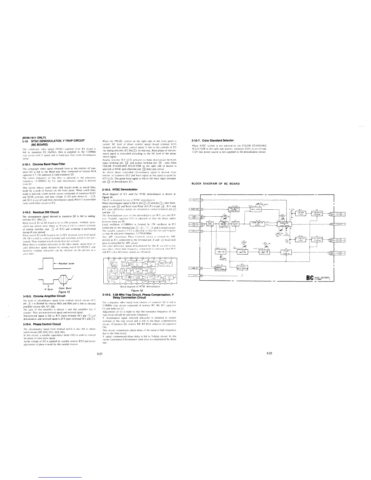
Block diagram of NTSC demodulator
Figure 16
3-10-6. 3.58 MHz Trap Circuit, Phasa Compensation Y
Delay Conrrection Circuit '
The rnmposite video si!!nal from emitter ut transistor QI is led to
3 58MHz trap circuit composed nf resistor RS. R6. R7. capacitor
CI and inductor L l.
Adjustment of L1 is made so that the resonance frequency of this
trap circuit should be subcarrier frequency.
Y I Luminance) signal removed subcarrier is obtained at output
terminal of the trar cirrnit and is fed to the phase compensation
circuit. !Transistor 02. resistor R8. R9 R 10. inductor L2 caracitor
C4)
This circuit compensates phase delay of the si~nal at high frequenc}·
due to the trap circuit.
Y siirnal •:ompensated phase delay is fed to Y-delay circuit. In this
circuit Luminancc/Chrominancc time error is compensated by delay
line.
3-10-7. Color Standard Selector
When NTSC system is not selected by the COLOR STANDARD
SI LITTOR in the riµht side drawer, transistor Ql O 1 is cut off and
+ 12V line power source is not supplied to the demodulator circuit.
BLOCK DIAGRAM OF BC BOARD
SC,·P
~
•OEO 11,(
-10[0 11,(
RfS P
,,,
(3111),
(6 l.8
(Hi:fOlilA AMl'LIF[R
•
euno1
.,.
''
,,
;'PULS[
(OIIR[CT
'°'
o,
Y·DE~jn •11i1E
'°'
q5 6 7_(, 2 .l•
Ra,9,,Q,L2,(4
~
'i8M.,, 1'11AP t---+---
O•CJ 04
ss,
'"
J
3-22
("'2
! 551,rn, OSC
l"ll[fllUN
( ~'
,:uAC
Pl'ISfal.OJ
"'
,.,
L[VfL
,o,
,,
YQi.,l8i.JtF
•
SYSTEM SW
O!S,20
o,,
IITCUl8UFF8
SYSTEM~
e r ov~ Burr e
~TO(t,I $#
,,,
"'
,,,
..
"
BC (NTSC DECODER)
_____________ Y.T_R_AP ____ .J
¥ OvT
T OvT
 Loading...