26 www.xilinx.com VC707 Evaluation Board
UG885 (v1.4) May 12, 2014
Chapter 1: VC707 Evaluation Board Features
A 2-mm JTAG header (J4) is also provided in parallel for access by Xilinx download cables
such as the Platform Cable USB II and the Parallel Cable IV.
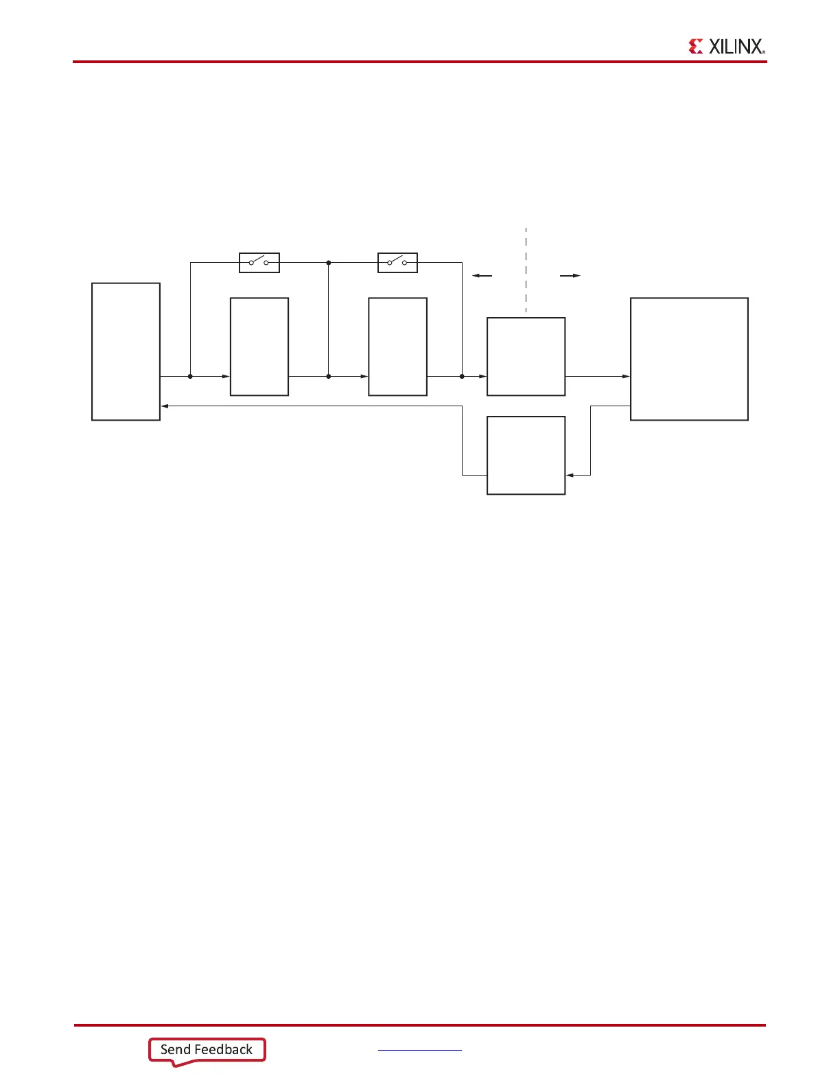
The JTAG chain of the VC707 board is illustrated in Figure 1-7. JTAG configuration is
allowed at any time regardless of FPGA mode pin settings. JTAG initiated configuration
takes priority over the configuration method selected through the FPGA mode pin settings
at SW11.
When an FMC mezzanine card is attached to the VC707 board it is automatically added to
the JTAG chain through electronically controlled single-pole single-throw (SPST) switches
U27 and U28. The SPST switches are in a normally closed state and transition to an open
state when an FMC mezzanine card is attached. Switch U27 adds an attached FMC1 HPC
mezzanine card to the FPGAs JTAG chain as determined by the
FMC_HPC_PRSNT_M2C_B signal. Switch U28 adds an attached FMC2 HPC mezzanine
card to the FPGAs JTAG chain as determined by the FMC2_LPC_PRSNT_M2C_B signal.
The attached FMC card must implement a TDI-to-TDO connection via a device or bypass
jumper to ensure that the JTAG chain connects to the FPGA U1.
The JTAG connectivity on the VC707 board allows a host computer to download
bitstreams to the FPGA using the Xilinx® iMPACT software. In addition, the JTAG
connector allows debug tools such as the Vivado serial I/O analyzer or a software
debugger to access the FPGA. The iMPACT software tool can also indirectly program the
Linear BPI Flash memory. To accomplish this, the iMPACT software configures the FPGA
with a temporary design to access and program the BPI memory device.
X-Ref Target - Figure 1-7
Figure 1-7: JTAG Chain Block Diagram
UG885_c1_07_021412
1.8V3.3V
FMC1 HPC
Connector
TDI
TDO
J35
USB
Module (U26)
or
JTAG
Connector
(J4)
TDO
TDI
U1
Kintex-7
FPGA
TDI
TDO
SN74AVC1T45
Voltage
Translator
TDI TDO
U46
FMC2 HPC
Connector
TDI
TDO
J37
SPST Bus Switch
U27
N.C. N.C.
SPST Bus Switch
U28
SN74AVC1T45
Voltage
Translator
TDO TDI
U72

 Loading...


