VC707 Evaluation Board www.xilinx.com 41
UG885 (v1.4) May 12, 2014
Feature Descriptions
The Ethernet connections from FPGA U1 to the 88E1111 PHY device are listed in
Table 1-18.
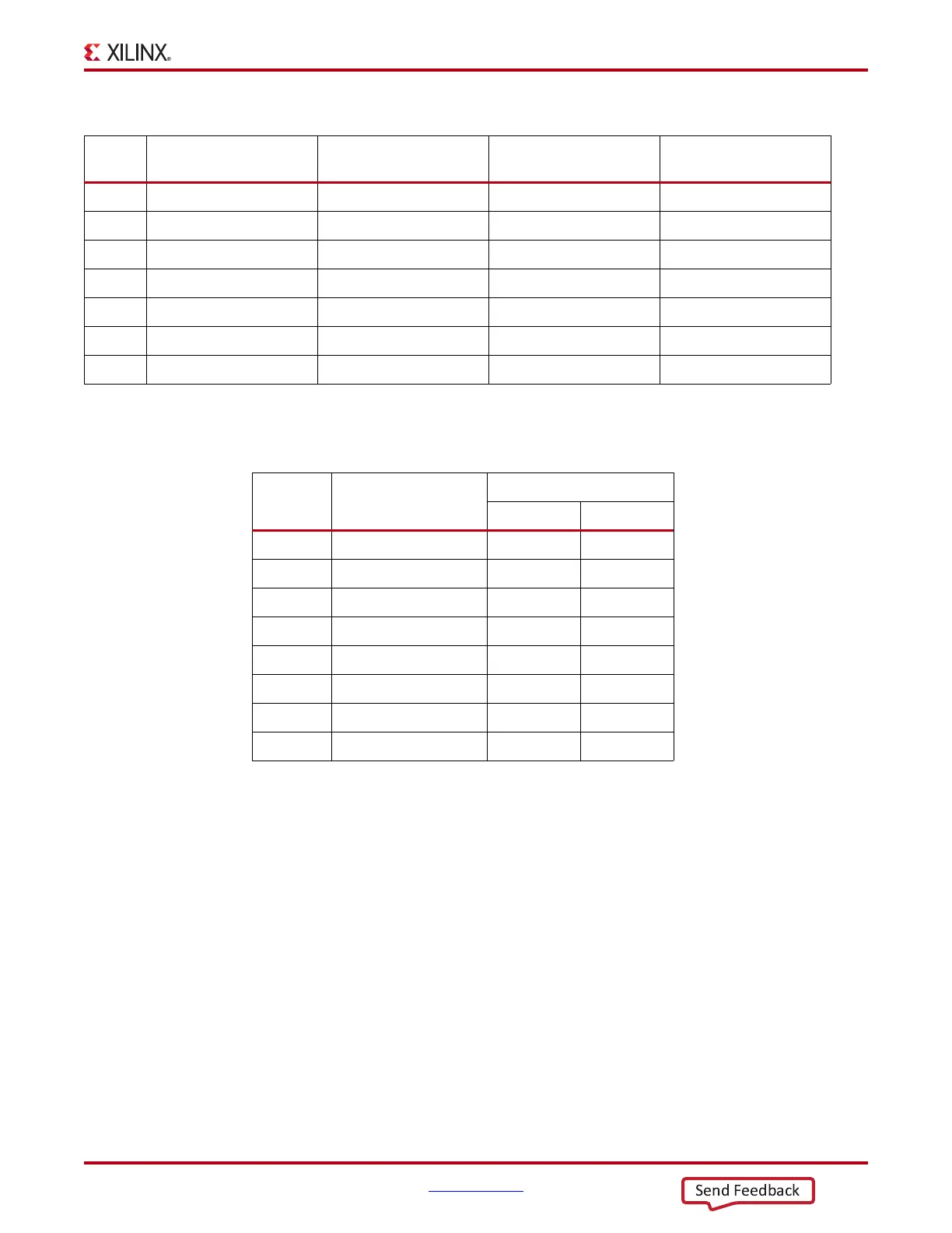
Table 1-17: Board Connections for PHY Configuration Pins
Pin Connection on Board
Bit[2]
Definition and Value
Bit[1]
Definition and Value
Bit[0]
Definition and Value
CFG0 V
CC
2.5V PHYADR[2] = 1 PHYADR[1] = 1 PHYADR[0] = 1
CFG1 Ground ENA_PAUSE = 0 PHYADR[4] = 0 PHYADR[3] = 0
CFG2 V
CC
2.5V ANEG[3] = 1 ANEG[2] = 1 ANEG[1] = 1
CFG3 V
CC
2.5V ANEG[0] = 1 ENA_XC = 1 DIS_125 = 1
CFG4 V
CC
2.5V HWCFG_MD[2] = 1 HWCFG_MD[1] = 1 HWCFG_MD[0] = 1
CFG5 PHY_LED_LINK10 DIS_FC = 1 DIS_SLEEP = 1 HWCFG_MD[3] = 1
CFG6 PHY_LED_RX SEL_BDT = 0 INT_POL = 1 75/50Ω= 0
Table 1-18: Ethernet Connections, FPGA to PHY Device
FPGA (U1)
Pin
Net Name
M88E1111 PHY U50
Pin Name
AK33 PHY_MDIO M1 MDIO
AH31 PHY_MDC L3 MDC
AL31 PHY_INT L1 INT_B
AJ33 PHY_RESET K3 RESET_B
AN2 SGMII_TX_P A3 SIN_P
AN1 SGMII_TX_N A4 SIN_N
AM8 SGMII_RX_P A7 SOUT_P
AM7 SGMII_RX_N A8 SOUT_N

 Loading...


