76 www.xilinx.com VC707 Evaluation Board
UG885 (v1.4) May 12, 2014
Chapter 1: VC707 Evaluation Board Features
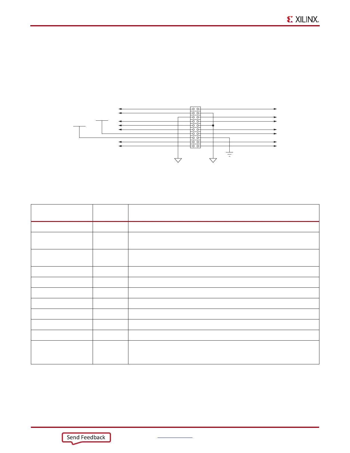
For external measurements an XADC header (J19) is provided. This header can be used to
provide analog inputs to the FPGA's dedicated VP/VN channel, and to the
VAUXP[0]/VAUXN[0], VAUXP[8]/VAUXN[8] auxiliary analog input channels.
Simultaneous sampling of Channel 0 and Channel 8 is supported.
A user-provided analog signal multiplexer card can be used to sample additional external
analog inputs using the 4 GPIO pins available on the XADC header as multiplexer address
lines. Figure 1-35 shows the XADC header connections.
Table 1-33 describes the XADC header J19 pin functions.
X-Ref Target - Figure 1-35
Figure 1-35: XADC Header (J19)
UG885_c1_32_030512
XADC_VP
XADC_VAUX0N
XADC_VAUX8P
XADC_DXN
XADC_VCC_HEADER
XADC_VN
XADC_VAUX0P
XADC_VAUX8N
XADC_DXP
XADC_VREF
XADC_GPIO_0
XADC_GPIO_2
XADC_GPIO_1
XADC_GPIO_3
J19
1
3
5
7
9
11
13
15
17
19
2
4
6
8
10
12
14
16
18
20
GND
XADC_AGNDXADC_AGND
XADC_VCC5V0
VADJ
Table 1-33: XADC Header J19 Pinout
Net Name
J19 Pin
Number
Description
VN, VP 1, 2 Dedicated analog input channel for the XADC.
XADC_VAUX0P, N 3, 6
Auxiliary analog input channel 0. Also supports use as I/O inputs when
anti-alias capacitor is not present.
XADC_VAUX8N, P 7, 8
Auxiliary analog input channel 8. Also supports use as I/O inputs when
anti-alias capacitor is not present.
DXP, DXN 9, 12 Access to thermal diode.
XADC_AGND 4, 5, 10 Analog ground reference.
XADC_VREF 11 1.25V reference from the board.
XADC_VCC5V0 13 Filtered 5V supply from board.
XADC_VCC_HEADER 14 Analog 1.8V supply for XADC.
VADJ 15 VCCO supply for bank which is the source of DIO pins.
GND 16 Digital Ground (board) Reference
XADC_GPIO_3, 2, 1, 0 19, 20, 17, 18
Digital I/O. These pins should come from the same bank. These I/Os should
not be shared with other functions because they are required to support 3-state
operation.

 Loading...


