ZCU111 Board User Guide 49
UG1271 (v1.1) August 6, 2018 www.xilinx.com
Chapter 3: Board Component Descriptions
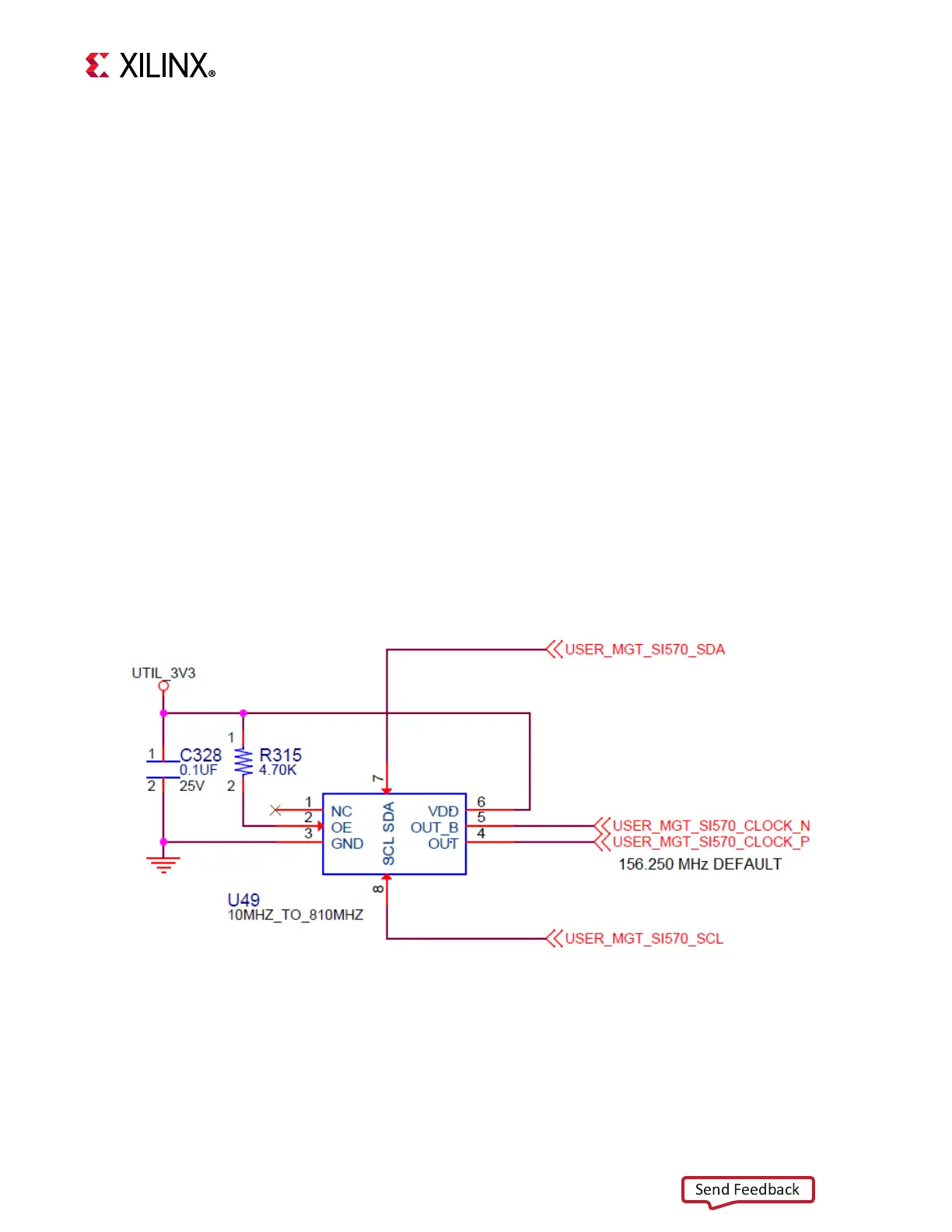
Programmable User MGT SI570 Clock
[Figure 2-1, callout 10]
The ZCU111 board has a programmable low-jitter 3.3V LVDS SI570 differential oscillator
(U49) connected to the XCZU28DR U1 GTY bank 129. The USER_MGT_SI570_CLOCK_P and
USER_MGT_SI570_CLOCK_N clock signals are connected through series capacitors to
XCZU28DR RFSoC U1 pins V31 and V32, respectively. At power-up, the user clock defaults to
an output frequency of 156.250 MHz. User applications can change the output frequency
within the range of 10 MHz to 810 MHz through an I2C interface. Power cycling the ZCU111
board reverts this user clock to the default frequency of 156.250 MHz.
This oscillator can be reprogrammed from MSP430 system controller U41 (see TI MSP430
System Controller, page 95 for more system controller information and the ZCU111 web
page for the tutorial on the system controller user interface (XTP517) [Ref 11].
• Programmable oscillator: Silicon Labs Si570BAB000544DG (10 MHz-810 MHz,
156.250 MHz default)
•LVDS differential output
• Total stability: 61.5 ppm
The programmable user clock MGT circuit is shown in Figure 3-15.
X-Ref Target - Figure 3-15
Figure 3-15: Programmable User MGT Clock

 Loading...


