101
Chapter 5 Theory of Operation
Digital Waveform, Pulse, and Sync
4
5
U1704 is a comparator driven by the 2.2 Vp-p signal from U1703 to
generate square waves. System DAC signal, V_THRESH, sets the duty
cycle of the square wave. The square wave output, SQUARE_DWF,
is sent to the SYNC selector (U1502) and the AND gate U1507-B where,
if it is enabled by SQUARE_DWF_EN being high, it is passed to the
Digital Waveform Translator.
Digital Waveform, Pulse, and Sync
See “A1 Digital Waveform and Sync Schematic” on page 199.
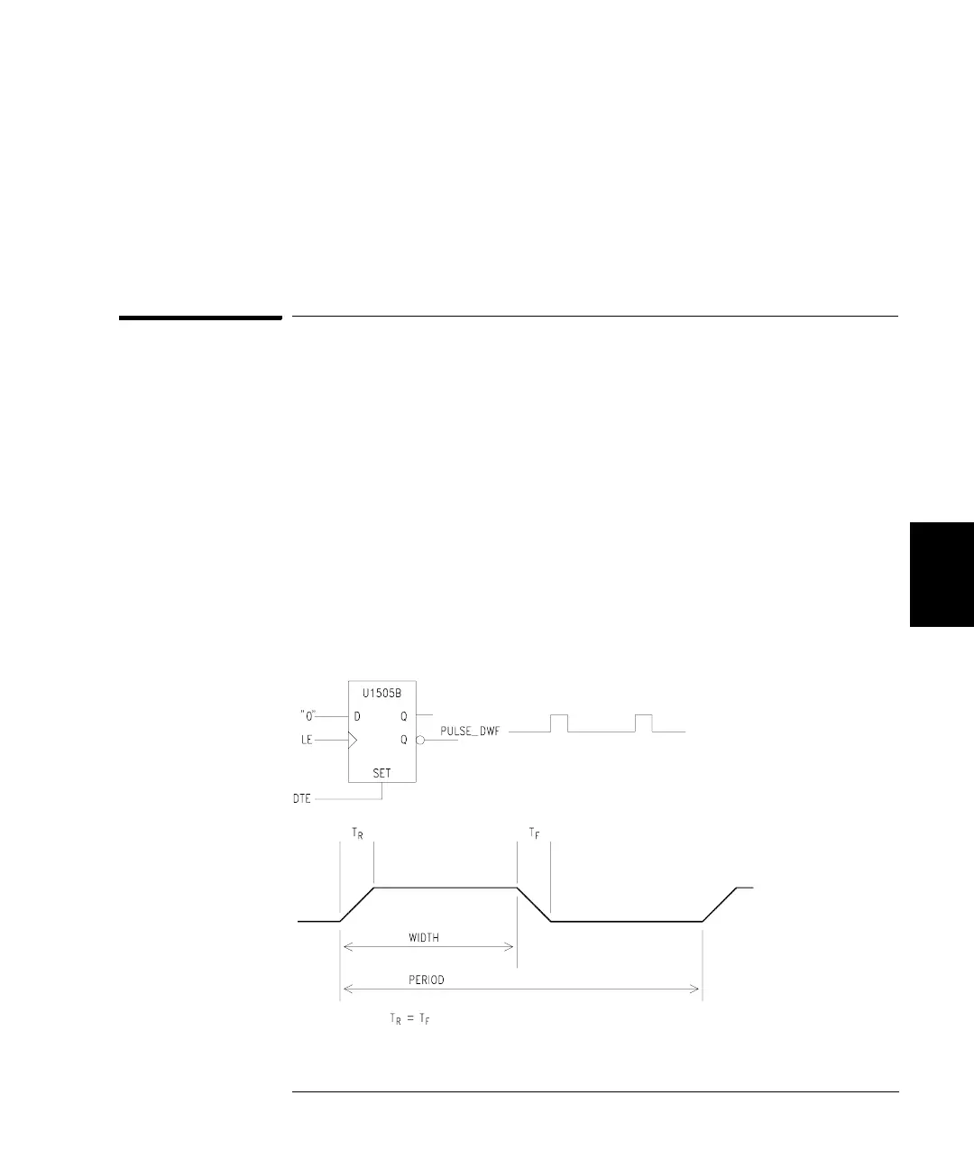
There are three timing parameters for pulse waveforms: period, width,
and leading/trailing edge time. At the beginning of each period, a short
pulse on LE clocks a “0” into flip-flop U1505-B to initiate the leading
edge on PULSE_DWF. Later, a short pulse on TE triggers a variable-
delay circuit consisting of U1505-A,U1506-A, U1507-D and associated
components. The output of the delay circuit, DTE, sets U1505-B to cause
the pulse’s trailing edge.
PULSE_DWF is the digital version of the pulse waveform. If U1507-A
is enabled (PULSE_DWF_EN is high), the signal is passed to the Digital
Waveform Translator, where leading- and trailing-edge times are
controlled.
 Loading...