8.1 Self-test and Error Message
8-2
2. TX/RX PCB
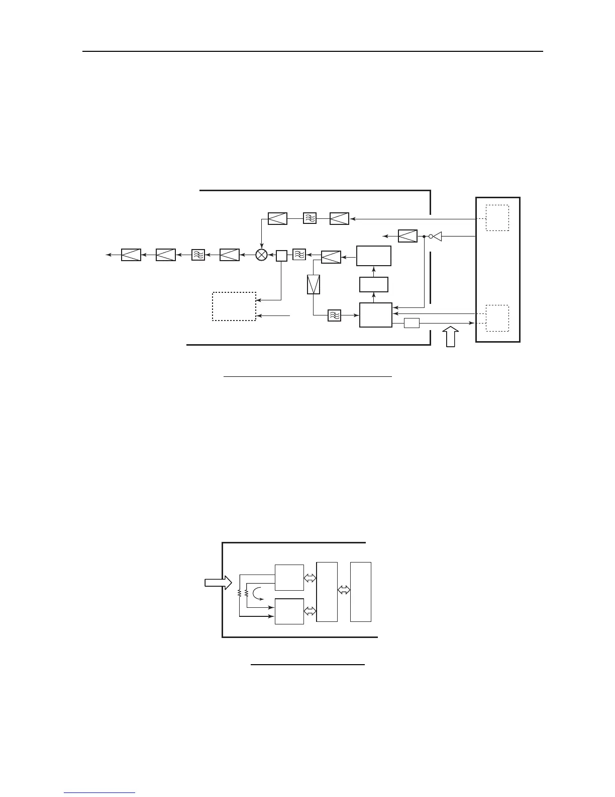
This is to check the unlocked state of PLL circuit on TX/RX board (05P0774A, B).
Frequency to be checked is the frequency set up at the time of self-test. The
Un-lock/Lock signal is outputted from U12: PLL IC on TX/RX board. PLL circuit on
this board is used with both TX and RX. Tx Local frequency is Fo + 45 MHz, and RX
Local frequency is Fo + 51.2375 MHz.
Fig. 8.1.2 TX/RX PLL Block Diagram
3. CPU PCB
This is a loop-back test where test signal is transmitted from U17: CODEC on CPU
board (05P0773) and is detected by U10: CODEC. A signal transmitted from U17 is
sine wave of 2 kHz. If this frequency and a designated level are detected by U10, it will
be assessed “OK’’. U25: DDS check is carried out the same way and a test signal is
transmitted from DDS. U17 digitizes (A/D conversion) IF signal of 37.5 kHz
transmitted from CH70 RX board, TX/RX board and DUP RX board. U10 on the other
hand, digitizes (A/D, D/A conversion) mainly LINE input/output and AF input/output
from a Remote Handset. Refer to page 8-16 for DDS/CODEC test which takes the same
procedure.
Fig. 8.1.3 CPU PCB Test
U17
(AK4528VF)
U10
(AK4543)
CODEC
CODEC
CPU
05P0773
DSP
U20
(ADSP2186)
CPU
U30
(HD64F2377)
AOUT R
VIDEO R
VIDEO L
AOUT L
R282
R283
2SK3874
2SC3356
PMBF M310
VCO
LPF
PLL
PLL1 UN-LOCK
RA35H1516M
RX
circuit
DRIVE BPF(L/C)
PMBF J310
ISS271
BPF(L/C)
TA4001
2SC3356
1SV229
51.2MHz
45 MHz
45 MHz
45 MHz
Rx 1st Lo
(Fo+51.2375MHz)
PLL1 DATA(STB/DATA/CLK)
PA
Tx out
U1 Q1,5
CR101
Q101
U10
U8
Q13
TA4001
U5
FL1: 45MHz
U12
LMX2353TMX
Q14, CR11/12
Q15
uPC2745TB
2SC3356
U7
uPC2745TB
Tx Local
(F0+45 MHz)
MIX
F0
Q21
U30
CPU
U25
DDS
CPU
05P0773
TX/RX
05P0774
U11
Q20
TC75HU04F
X2
25.6MHz
Rx 2nd Lo
(51.2MHz)
Rx 2nd Lo
(51.2MHz)
Ref. OSC
SW
 Loading...