2-7
2
3
4
4
6
7
8
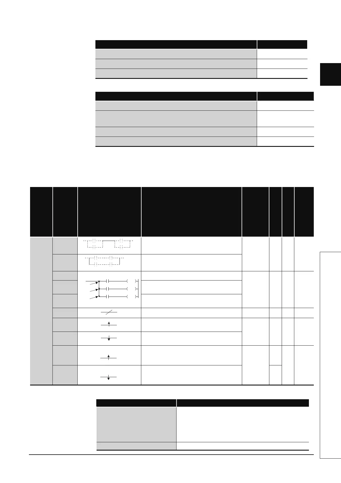
2.3 Sequence Instructions
2.3.2 Association instructions
*2: The number of steps may vary depending on the device and type of CPU module being used.
The number of steps may vary depending on the device being used.
2.3.2 Association instructions
Table 2.4 Association Instructions
*1: The number of steps may vary depending on the device and type of CPU module being used.
Device Number of Steps
Internal device, file register (R0 to R32767)
1
Direct access input (DX)
1
Devices other than above
3
Device Number of Steps
Internal device, file register (R0 to R32767)
Number of Basic Steps
Serial number access format file register (ZR), Extended data register (D),
Extended link register (W), Multiple CPU shared device (U3En\G10000)
Number of Basic Steps +1
Direct access input (DX)
Number of Basic Steps +1
Devices other than above
Number of Basic Steps +2
Category
Instruction Symbol
Symbol Processing Details
Execution
Condition
Number of Basic Steps
Subset
See for Description
Connec-
tion
ANB
• AND between logical blocks
(Series connection between logical blocks)
1 - 5-10
ORB
• OR between logical blocks
(Series connection between logical blocks)
MPS • Memory storage of operation results
1 - 5-12
MRD
• Read of operation results stored with MPS
instruction
MPP
• Read and reset of operation results stored with
MPS instruction
INV • Inversion of operation result
1 - 5-15
MEP
• Conversion of operation result to leading edge
pulse
1 - 5-17
MEF
• Conversion of operation result to trailing edge
pulse
EGP
• Conversion of operation result to leading edge
pulse
(Stored at Vn)
1
-5-18
EGF
• Conversion of operation result to trailing edge
pulse
(Stored at Vn)
*1
Component Number of Basic Steps
High Performance model QCPU
Process CPU
Redundant CPU
Universal model QCPU
LCPU
1
Basic model QCPU
2
ANB
ORB
MPS
MRD
MPP
Vn
Vn
 Loading...