June 15, 2005 6815854H01-A
4-28 Troubleshooting Procedures: Standard Bias Tables
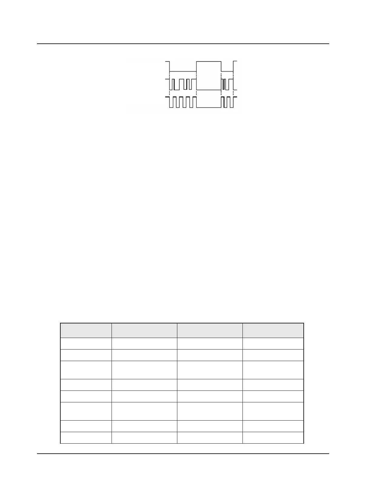
Figure 4-12. Waveform Representation During Programming of the LV Frac-N IC (U6751)
NOTE: The above waveforms are representations only.
4.9.3 No or Low Output Power (TX or RX Injection)
In addition to the schematic and theory of operation, refer to the transmitter injection troubleshooting
flowchart and the receiver injection trouble shooting flowchart in Chapter 5. The charts will guide you
through a sequence of tests and checks designed to isolate problems in the Transmitter or receiver
injection strings.
4.9.4 No or Low Modulation
In addition to the schematic and theory of operation, refer to the transmitter no TX Audio
troubleshooting flowchart in Chapter 5. The chart will guide you through a sequence of tests and
checks designed to isolate problems in the Transmitter Audio section of the FGU.
4.9.5 Troubleshooting the Back-End
Refer to “5.6.36 RX Back-End—Poor SINAD or No Audio (700–800 MHz)—Part 1 of 3” on page 5-
47.
4.10 Standard Bias Tables
Table 4-16, below, outlines some standard supply voltages and system clocks that should be present
during normal operation. These should be checked as a first step to any troubleshooting procedure.
Table 4-16. Standard Operating Bias: Power Lines
Nominal Value Signal Name Range/State Probe Locations
13.8 V A+ (at DC connector) 11.0 to 16.6 V J0401-20, TP0414
13.8 V IGNITION 11.0 to 16.6 V J0401-19, J0401-21
13.8 V SW_A+
(on board only)
11.0 to 16.6 V U0500-4, Q0503
13.8 V SW_B+ (from C.H.) 11.0 to 16.6 V TP0413, J0401-17
2.83 V SW_B+_SENSE No change U0604-7
2.5 V SW_B+_ON_OFF
(on board only)
2 to 3 V Q0505-1, Q0504-1
9.1 V 9.3V_ABACUS No change U0505-1
9.1 V 9.3V No change TP0951, TP0950
Pin 9 (Chip Select)
Pin 7 (Data)
Pin 8 (Clock)
MAEPF-27805-O

 Loading...