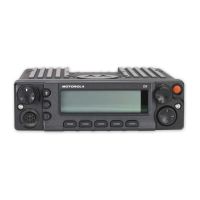
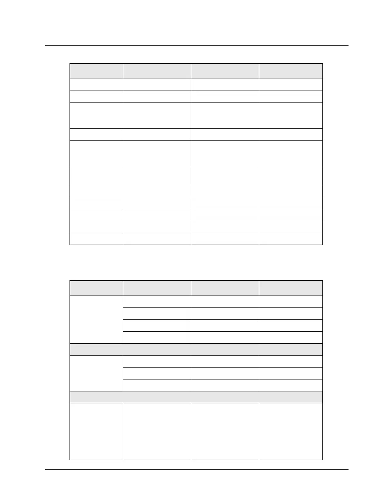
6815854H01-A June 15, 2005
Troubleshooting Procedures: Standard Bias Tables 4-29
.
9.18 V 9V No change U0500-5
5 V 5V_ABACUS No change U0505-3
5 V VCC_5 No change J0401-23, U0507-8,
U0503-3, U0502-8,
U0501-8
3 V VCC_3 No change U0962-5
2.85 V LV_DETECT When A+ drops too far
below 9 V, this line goes
to 0 V
U0504-1
2.85 V STO
(at microprocessor)
No change TP0500
2.85 V VCC_2.85 No change U0501-1
1.86 V Vpp No change TP0400
1.85 V VCC_1.8 1.84 to 1.87 V U0507-1
1.55 V VCC_1.55 No change U0502-1
1.42 V VAG No change U0206-1, U0201-3
Note: Do not KEY UP unless the board is inside a chassis.
Table 4-17. Standard Operating Bias: Clock and Control Lines
Nominal Value Signal Name Range/State Probe Locations
(See “Chapter 6
Troubleshooting
Waveforms” on
page 6-1)
SB9600__BUS + Idle=High (4 V to 5 V) J0402-3, J2-2
SB9600__BUS - Idle=Low (0 V) J0402-5, J2-3
SB9600__BUSY Idle=Low (0 V) J0402-4, J2-9
SB9600__RESET Idle=Low (0 V) J0402-6, J2-8
Note: Use chassis as GND when measuring on an oscilloscope.
(See “Chapter 6
Troubleshooting
Waveforms” on
page 6-1)
USB_PWR 5.1 V J0402-12, J2-12
USB_DATA + J0402-11, J2-7
USB_DATA - J402-13, J2-6
Note: Use chassis as GND when measuring on an oscilloscope.
(See “Chapter 6
Troubleshooting
Waveforms” on
page 6-1)
RS232__UARTA_TX Output voltage level is
the same as BOOT TX
TP0407, J2-7
RS232__UARTA_RX Input level depends on
inputting device's levels
TP0408, J2-9
RS232__UARTA_CTS Flow control line—not
used always
TP0409, J2-8
Table 4-16. Standard Operating Bias: Power Lines (Continued)
Nominal Value Signal Name Range/State Probe Locations

 Loading...