2. Assembly
2.1 General guidelines
Assembly of this kit is quite straightforward, but very detailed; most components are SMD and
have already been pre-assembled by the PCB factory. The usual kit-building recommendations
apply: work in a well-lit area, with peace and quiet to concentrate. Some of the other
semiconductors in the kit are sensitive to static discharge. Therefore, observe Electrostatic
discharge (ESD) precautions.
And I say it again: FOLLOW THE INSTRUCTIONS!!
Don’t try to be a hero and do it without instructions!
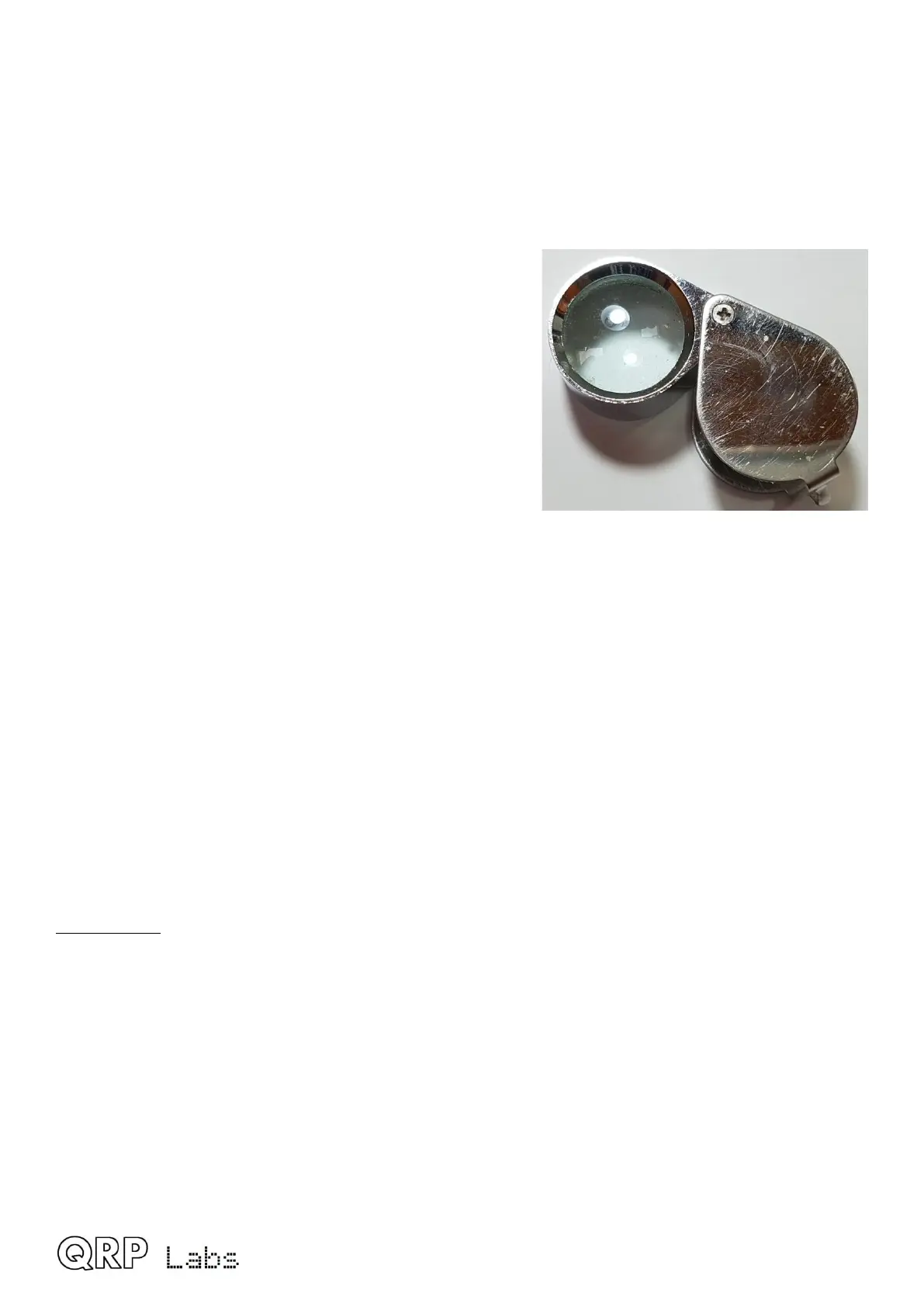
A jeweler's loupe is really useful for inspecting small
components and soldered joints. You’ll need a fine-
tipped soldering iron too. It is good to get into the habit of
inspecting every joint with the magnifying glass or
jeweler's loupe (like this one I use), right after soldering.
This way you can easily identify any dry joints or solder
bridges, before they become a problem later on when
you are trying to test the project.
You could also take photos with a mobile phone, and use the phone’s zoom features to view the
board in detail.
Triple check every component value and location BEFORE soldering the component!
It is easy to put component leads into the wrong holes, so check, check and check again! It is
difficult to de-solder and replace components, so it is much better to get them correctly installed
the first time. In the event of a mistake, it is always best to detect and correct any errors as early
as possible (immediately after soldering the incorrect component). Again, a reminder: removing a
component and re-installing it later is often very difficult! This is particularly true on this QMX
design where the components must be installed very close together.
Please refer to the layout diagram and PCB tracks diagrams below, and follow the steps carefully.
Use of a good quality soldering iron and solder is highly recommended for best results!
The following diagrams show the PCB layout and track diagrams of the QMX.
6-layer PCB
QMX is a 6-layer PCB. This means that there are two internal ground-planes and two internal
signal layers, in addition to the normal top and bottom signal layers. This is necessary in order to
achieve the required component density in the QMX design, as well as to achieve the required
ground-plane, signal ground return paths necessary to deliver low-noise and high performance
with such a high component density in a mixed mode (analog/digital) board.
Because of the internal layers it is essential that you never ever drill into the PCB; just
because you think you see a clear spot on the top and bottom layers, does NOT mean that
there is nothing hidden in the middle.
There should never be any reason to drill into the board anyway but I’m just saying, in case for
some peculiar reason you feel an irresistible temptation to go wild.
QMX assembly Rev 1.00e 5
 Loading...