Renesas RA Family RA4 Quick Design Guide
R01AN5988EU0100 Rev.1.00 Page 15 of 51
Jul.21.21
4.1 Option Setting Memory Registers
Following is a summary of the Option Setting Memory registers. Make sure that they are configured properly
before startup.
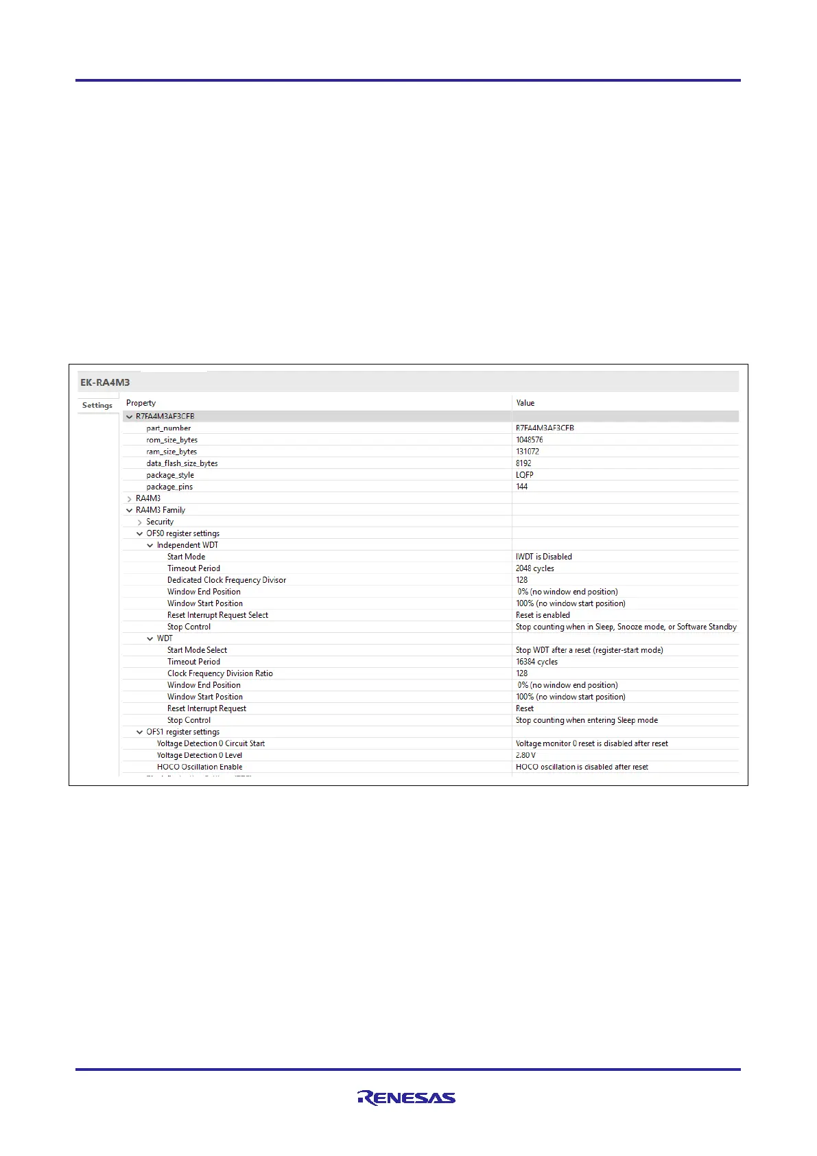
• OFS0 register
Independent Watchdog Timer (IWDT) auto start
IWDT timeout, frequency, windowing, interrupt type, and low power mode behavior
Watchdog Timer (WDT) auto start
WDT timeout, frequency, windowing, and interrupt type
• OFS1 register
LVD0 enable after reset
HOCO startup after reset
Renesas FSP Configurator supports setting of option memory in BSP settings, as shown in the following
figure for RA4M3 MCU. The settings made through the FSP configurator are reflected in the binary file
compiled to operate on the MCU.
Figure 10. Option Memory Settings in FSP Configuration for RA4M3 MCU
5. Clock Circuits
The RA4 MCUs have six primary oscillators. Five of these may be used as the source for the main system
clock. The remaining oscillator is dedicated to the Independent Watchdog Timer. In a typical system, the
main clock is driven with an external crystal or clock. This input is directed to the PLL where it is multiplied up
to the PLL clock, then post-divided down into the main system clock (ICLK), flash clock, peripheral module
clocks, external bus clock, trace clock, and USB clock. The ICLK is further used for the CPU clock, DMAC
clock, internal flash clock and SDRAM clock. Refer to the Hardware User’s Manual “Clock Generation
Circuit” chapter for the block diagram of the clock generation circuit.
Each clock has specific tolerances and timing values. Refer to the Hardware User’s Manual “AC
Characteristics” section in the “Electrical Characteristics” chapter for the Frequency and Clock Timing
specifications. Refer to the Hardware User’s Manual “Clock Generation Circuit” chapter for the relationship
between the various clock frequencies.

 Loading...


